Solar cell

Inactive Publication Date: 2015-02-26
HITACHI LTD
View PDF0 Cites 13 Cited by
  • Summary
  • Abstract
  • Description
  • Claims
  • Application Information

AI Technical Summary

Benefits of technology

[0022]Among embodiments of the present invention disclosed in this application, a brief summary of an advantageous effect obtained by some representatives is as f

Problems solved by technology

Transmission loss and quantum loss occupy a large proportion of a loss of a solar cell.
The transmission loss is a loss generated due to transmission of light having energ

Method used


Image

  • Solar cell
  • Solar cell
  • Solar cell

Examples


example 1

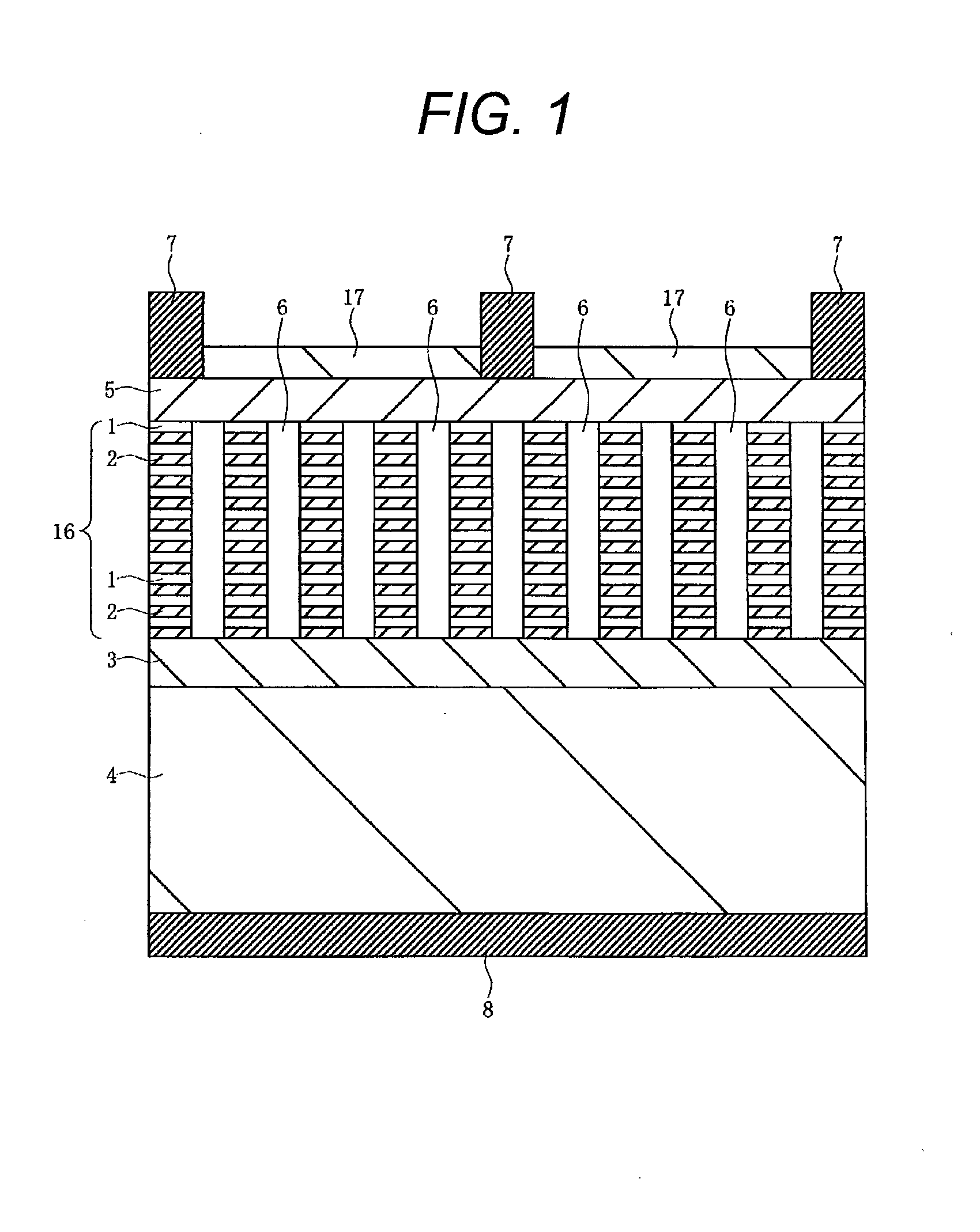
[0064]A solar cell according to Example 1 of the present invention is described with reference to a cross-sectional view of relevant parts of a solar cell illustrated in FIG. 1.

[0065]The feature of the structure of the solar cell according to Example 1 is to include a nanopillar array including a plurality of nanopillars (hereinafter, referred to as Si / SiGe nanopillars) constituted with a Si / SiGe superlattice including Si layers 1 and SiGe layers 2 laminated in an alternate manner arranged in a two-dimensional array on a primary surface of a p-type semiconductor substrate 4.

[0066]For example, a p-type semiconductor layer 3 is formed on the primary surface (front surface, first surface) of the p-type semiconductor substrate 4 formed of a Si single crystal. An impurity concentration of the p-type semiconductor layer 3 is higher than that of the semiconductor substrate 4, which is, for example, about 1018 cm−3 to 1020 cm−3. The p-type semiconductor layer 3 can be formed by an impurity ...

example 2

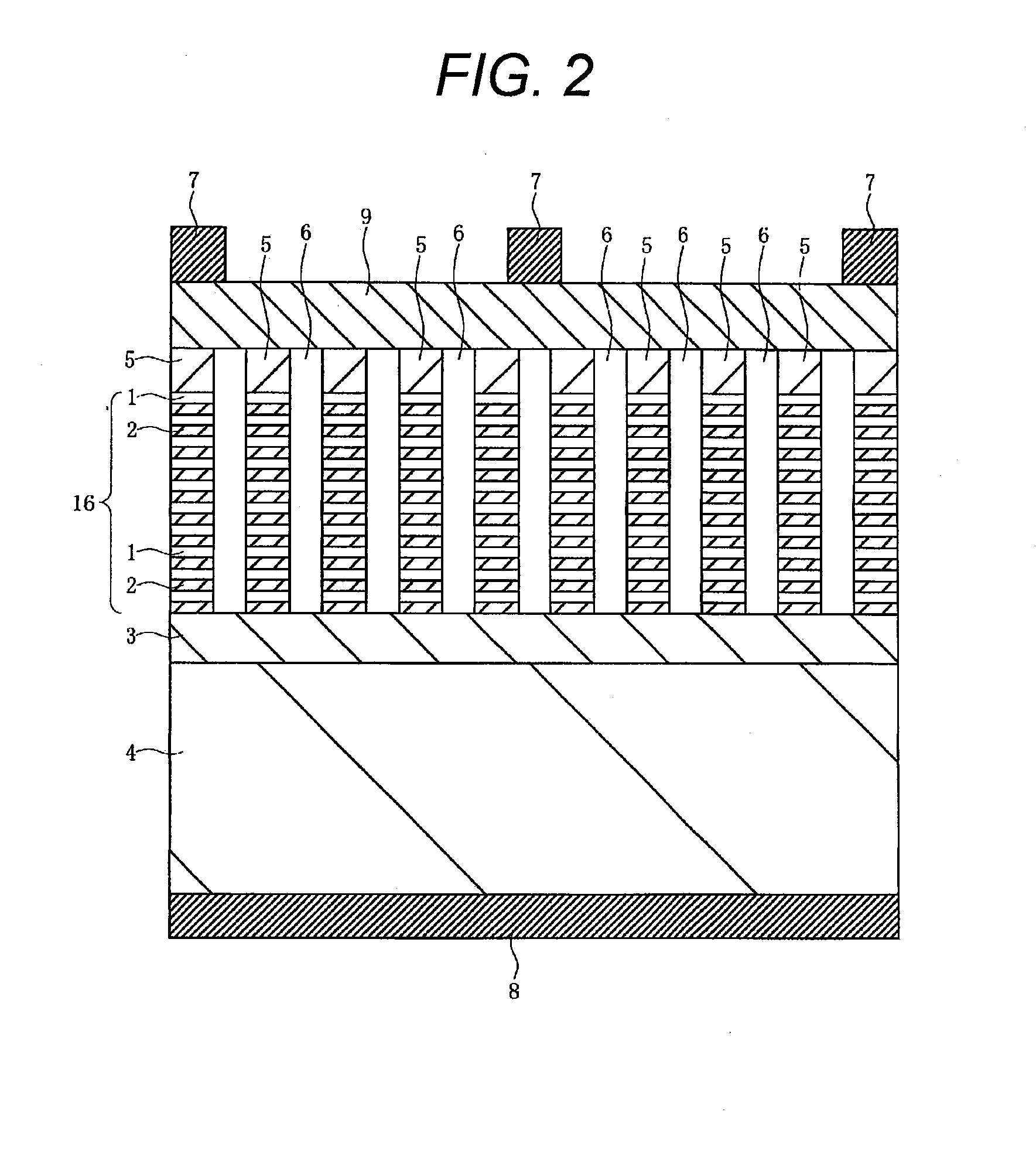
[0081]In the above-mentioned solar cell according to Example 1, the n-type semiconductor layer 5 is formed on the entire surface of the nanopillar array area 16 (nanopillar array and the inter-layer insulation film 6). In contrast to this, in a solar cell according to Example 2 of the present invention, an n-type semiconductor layer 5 is formed only on upper surfaces of the plurality of Si / SiGe nanopillars, and the n-type semiconductor layer 5 and a front surface electrode 7 are electrically connected to each other via a transparent conductive film 9 formed on the n-type semiconductor layer 5. The solar cell according to Example 2, which is configured in this manner, is described with reference to a cross-sectional view of relevant parts of the solar cell illustrated in FIG. 2.

[0082]In the similar manner to the above-mentioned example 1, for example, a p-type semiconductor layer 3 is formed on the primary surface of a p-type semiconductor substrate 4 formed of a Si single crystal.

[0...

example 3

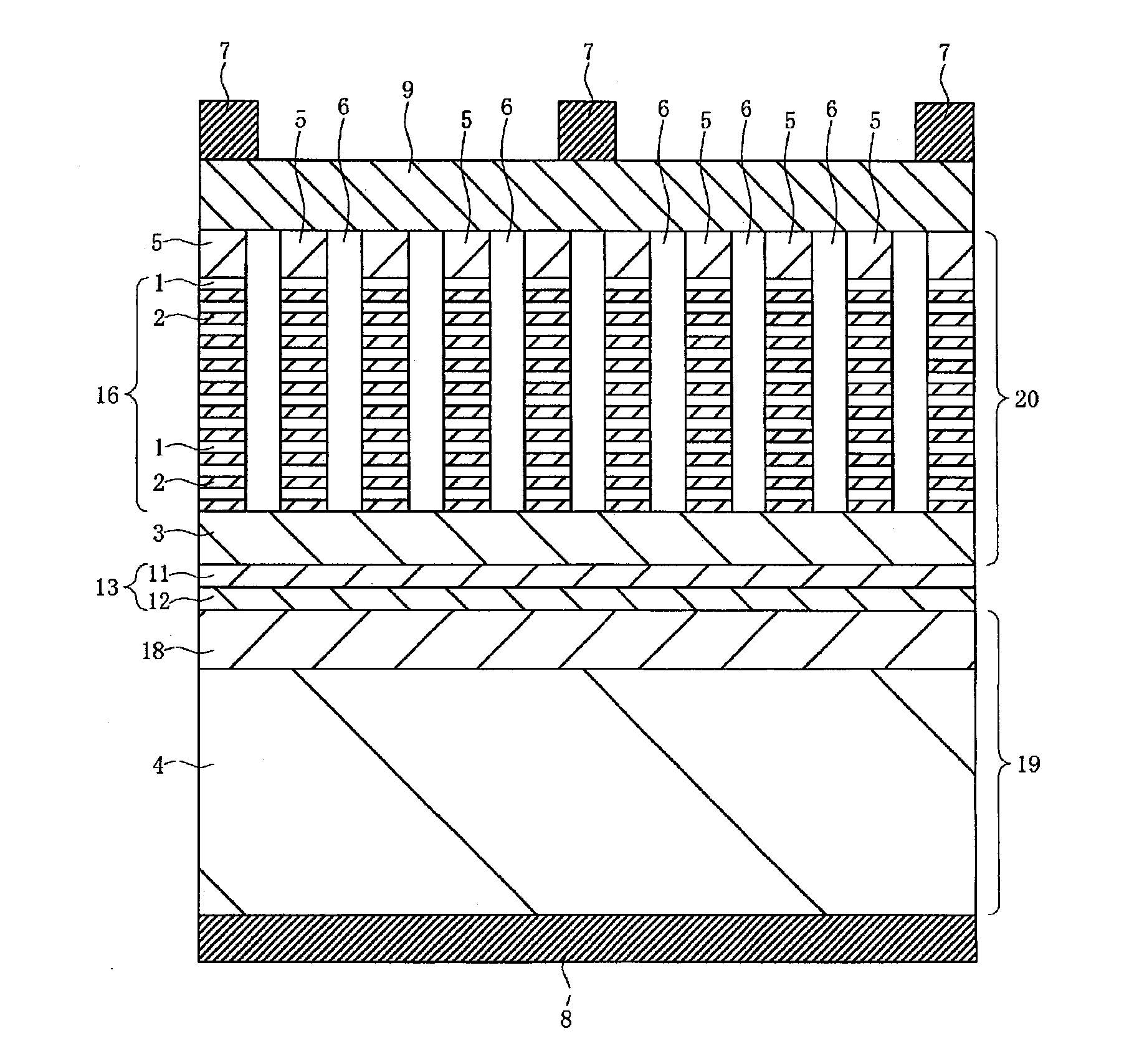
[0093]In Example 3 of the present invention, a modification example of the solar cell according to the above-mentioned example 1 is described. In the solar cell according to the above-mentioned example 1, the p-type semiconductor layer 3 is formed on the p-type semiconductor substrate 4. In contrast to this, in a solar cell according to Example 3, an n-layer semiconductor layer 18 having an impurity concentration higher than that of the p-type semiconductor substrate 4 and a tunnel junction layer 13 including an p-layer semiconductor layer 11 and a p-type semiconductor layer 12 are formed between a p-type semiconductor substrate 4 and a p-type semiconductor layer 3. The solar cell according to Example 3 configured in this manner is described with reference to a cross-sectional view of relevant parts of the solar cell illustrated in FIG. 3.

[0094]For example, the n-type semiconductor layer 18 having an impurity concentration higher than that of the p-type semiconductor substrate 4 is ...


PUM


Abstract

A surface reflectivity of a solar cell is reduced by applying a nanopillar array including a plurality of nanopillars to the solar cell. Further, by constituting the nanopillars with a Si/SiGe superlattice and controlling a Ge composition ratio of a SiGe layer (2), excited electron and hole are spatially separated in different layers, thus increasing a carrier lifetime, and at the same time, an optical-electrical conversion efficiency is improved by a multi-exciton phenomenon due to a quantum confinement effect. In addition, by forming an intermediate band by thinning a Si layer (1) and the SiGe layer (2), a carrier extraction efficiency is improved.

Description

TECHNICAL FIELD[0001]The present invention relates to a solar cell, and more particularly, to a technology to be effectively applied to a solar cell using a superlattice structure (super structure and ordered lattice structure).BACKGROUND ART[0002]Transmission loss and quantum loss occupy a large proportion of a loss of a solar cell. The transmission loss is a loss generated due to transmission of light having energy smaller than a bandgap of material constituting the solar cell through the material without being absorbed by the material among solar light inputted to the solar cell. On the other hand, among the inputted solar light, light having energy larger than the bandgap of the material constituting the solar cell is absorbed inside the solar cell to generate a carrier. However, a surplus energy exceeding the bandgap is dissipated as a heat. This is the quantum loss. When the solar energy is assumed to be 100%, each of the transmission loss and the quantum loss takes about 20% ...

Claims


Application Information

Patent Timeline
IPC IPC(8): H01L31/0352H01L31/0328
CPCH01L31/035254H01L31/0328H01L31/035227B82Y20/00H01L31/0682H01L31/0687Y02E10/544Y02E10/547
Inventor TSUCHIYA, RYUTAWATANABE, KEIJIHATTORI, TAKASHIMATSUMURA, MIEKO
Owner HITACHI LTD
Why Eureka
Try Eureka