Semiconductor laser element

Pending Publication Date: 2021-06-03
NUVOTON TECH CORP JAPAN
View PDF0 Cites 0 Cited by
  • Summary
  • Abstract
  • Description
  • Claims
  • Application Information

AI Technical Summary

Benefits of technology

[0015]With the present disclosure, it is possible to provide a semiconductor laser ele

Problems solved by technology

This decreases the effect of confining light in the active la

Method used


Image

  • Semiconductor laser element
  • Semiconductor laser element
  • Semiconductor laser element

Examples


Example

Embodiment 1

[0045]A semiconductor laser element according to Embodiment 1 will be described.

[0046][1.-1. Overall Structure]

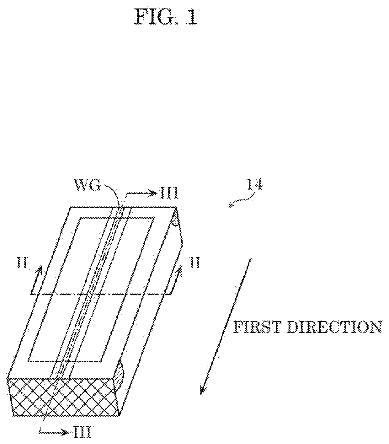
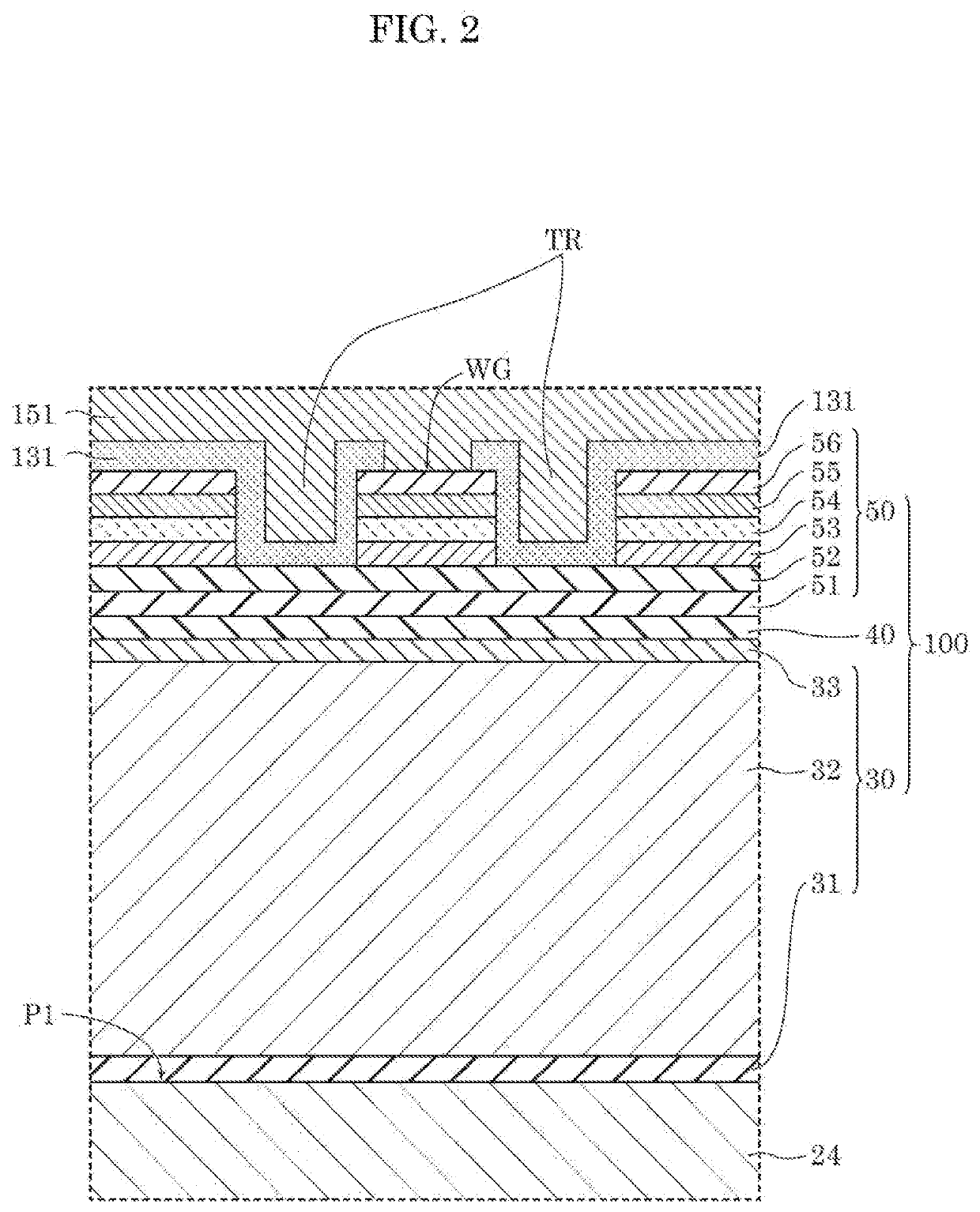
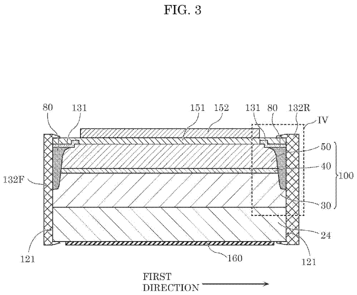
[0047]Firstly, the overall structure of a semiconductor laser element according to the present embodiment will be described with reference to FIG. 1 through FIG. 4.

[0048]FIG. 1 is a perspective view schematically illustrating the exterior of semiconductor laser element 14 according to the present embodiment. FIG. 2 is the first sectional view schematically illustrating the structure of semiconductor laser element 14 according to the present embodiment. FIG. 2 shows an enlarged sectional view of the vicinity of the waveguide WG taken along II-II of FIG. 1. FIG. 3 is the second sectional view schematically illustrating the structure of semiconductor laser element 14 according to the present embodiment. FIG. 3 shows the sectional view taken along III-III of FIG. 1. FIG. 4 is a partially enlarged view of FIG. 3. FIG. 4 shows an enlarged view of the IV part surrounde...

Example

Embodiment 2

[0133]A semiconductor laser element according to Embodiment 2 will be described. The semiconductor laser element according to the present embodiment mainly differs in the structure of an active layer from semiconductor laser element 14 according to Embodiment 1. The following describes the semiconductor laser element according to the present embodiment with reference to FIG. 14 and FIG. 15, mainly in terms of differences from semiconductor laser element 14 according to Embodiment 1.

[0134]FIG. 14 is a table illustrating the layer structure of the semiconductor laser element according to the present embodiment. FIG. 15 is a diagram illustratingthe energy band structure and the refractive index distribution of the semiconductor laser element according to the present embodiment. As shown in FIG. 15, the semiconductor laser element according to the present embodiment includes chip-like substrate 224, first semiconductor layer 230, active layer 240, and second semiconductor l...

Example

Embodiment 3

[0139]A semiconductor laser element according to Embodiment 3 will be described. The semiconductor laser element according to the present embodiment mainly differs in the structure of an active layer from semiconductor laser element 14 according to Embodiment 1. The semiconductor laser element according to the present embodiment can implement TM-mode oscillation. The following describes the semiconductor laser element according to the present embodiment with reference to FIG. 16 and. FIG. 17, mainly in terms of differences from semiconductor laser element 14 according to Embodiment 1.

[0140]FIG. 16 is a table illustrating the layer structure of the semiconductor laser element according to the present embodiment, FIG. 17 is a diagram illustrating the energy band structure and the refractive index distribution of the semiconductor laser element according to the present embodiment. As shown in FIG. 17, the semiconductor laser element according to the present embodiment inclu...


PUM


Abstract

A semiconductor laser element includes: an n-type cladding layer disposed above an n-type semiconductor substrate (a chip-like substrate); an active layer disposed above the n-type cladding layer; and a p-type cladding layer disposed above the active layer, in which the active layer includes a well layer and a barrier layer, an energy band gap of the barrier layer is larger than an energy band gap of the n-type cladding layer, and a refractive index of the barrier layer is higher than a refractive index of the n-type cladding layer.

Description

CROSS REFERENCE TO RELATED APPLICATIONS[0001]This application is a U.S. continuation application of PCT International Patent Application Number PCT / JP2019 / 027857 filed on Jul. 16, 2019, claiming the benefit of priority of Japanese Patent Application Number 2018-141109 filed on Jul. 27, 2018, the entire contents of which are hereby incorporated by reference.BACKGROUND1. Technical Field[0002]The present disclosure relates to a semiconductor laser element,2. Description of the Related Art[0003]Conventionally, a semiconductor laser element has been known as a small high-power light source (for example, see WO 2002 / 21578, etc.). In the design of such a semiconductor laser element, there is a demand for reduction in operating voltage to reduce power consumption or the like. In order to reduce the operating voltage, the semiconductor laser element disclosed in WO 2002 / 21578 is configured to have a larger energy band gap in a barrier layer included in an active layer than in an n-type cladd...

Claims


Application Information

Patent Timeline
IPC IPC(8): H01S5/32H01S5/20H01S5/343H01S5/02H01S5/22
CPCH01S5/3216H01S5/2009H01S5/22H01S5/0206H01S5/2031H01S5/34313H01S5/3211H01S5/34366H01S5/3436H01S2301/173H01S5/2004H01S5/162H01S5/028H01S5/1064
Inventor NAKATANI, TOUGOHATA, MASAYUKI
Owner NUVOTON TECH CORP JAPAN
Why Eureka
Try Eureka