Nitride semiconductor device and method of manufacturing the same

A nitride semiconductor and semiconductor technology, which is applied in the structure of semiconductor lasers, optical waveguide semiconductors, ion implantation and plating, etc., can solve the problems of affecting the optical characteristics of the device, complicating the process, and decreasing the yield, and achieves restraining electrode peeling. , high output, heat reduction effect

Inactive Publication Date: 2009-05-27
MITSUBISHI ELECTRIC CORP
View PDF2 Cites 2 Cited by
  • Summary
  • Abstract
  • Description
  • Claims
  • Application Information

AI Technical Summary

Problems solved by technology

[0006] However, in the method of Patent Document 1, since the materials of the insulating film and the adhesive layer are greatly different, there are problems in that the manufacturing process of the device is complicated, and in addition, the optical characteristics of the device are affected, causing a decrease in yield. reason
In the method of Patent Document 2, there is also a problem that the process of device fabrication is complicated

Method used


Image

  • Nitride semiconductor device and method of manufacturing the same
  • Nitride semiconductor device and method of manufacturing the same
  • Nitride semiconductor device and method of manufacturing the same

Examples


Embodiment approach 1

[0021] (structure)

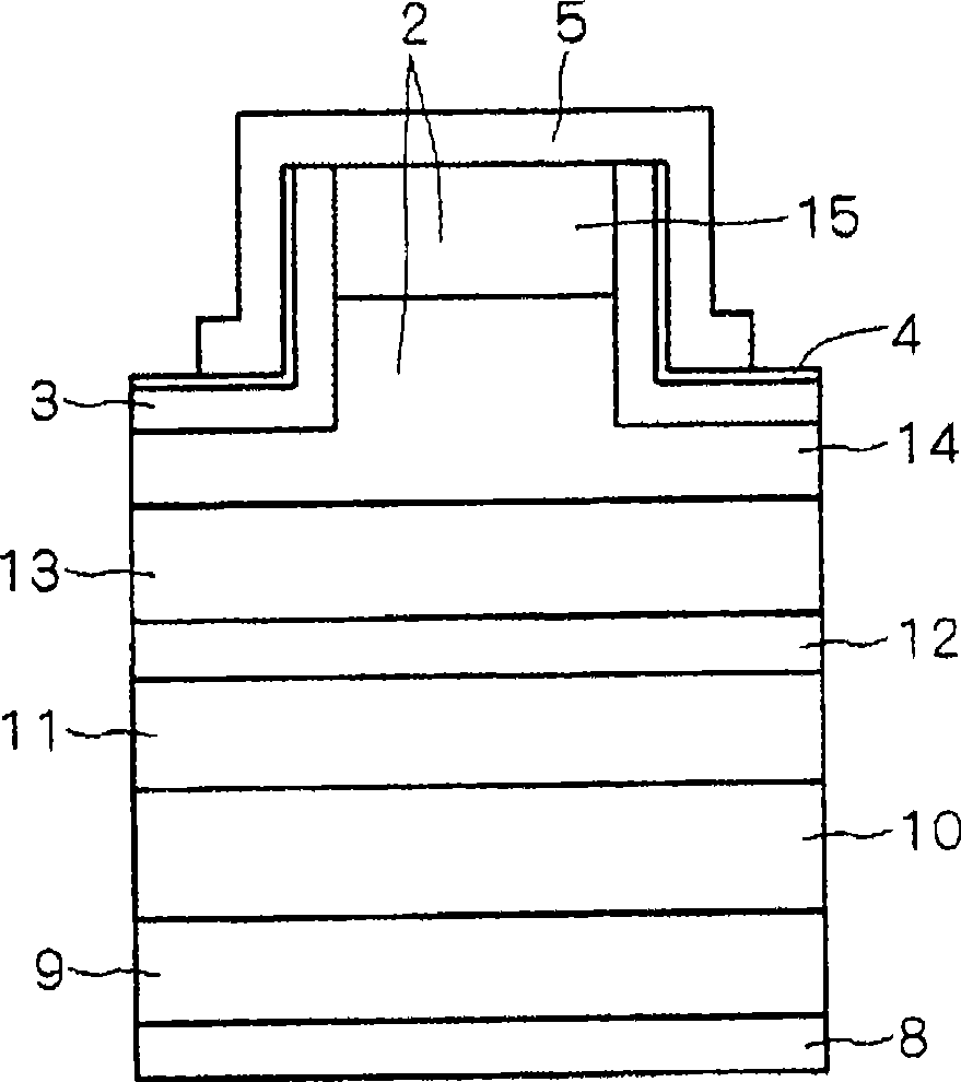
[0022] figure 1 It is a cross-sectional view showing main parts of the nitride semiconductor device of this embodiment. A ridge 2 is formed on the upper surface of a P-type nitride semiconductor layer (P-type semiconductor layer) 1 made of a P-type nitride semiconductor, and a ridge 2 is formed from the side surface of the ridge 2 to the top of the P-type nitride semiconductor layer 1 connected to the lower part of the side surface. surface, set SiO in turn in a covering manner 2 film (insulating film) 3, an Si adhesive layer (adhesive layer) 4 made of silicon, and a P-type electrode ( Electrode) 5.

[0023] also, figure 2 is showing figure 1 A cross-sectional view of a light-emitting nitride semiconductor device as an example of the whole of the nitride semiconductor device shown. The n-electrode 8, the n-GaN substrate 9, the n-AlGaN cladding layer 10, the n-GaN guiding layer 11, the active layer 12, the P-GaN guiding layer 13, the P-AlGaN cladding...

Embodiment approach 2

[0036] (structure)

[0037] Figure 7It is a cross-sectional view showing main parts of the nitride semiconductor device of this embodiment. A ridge 2 is formed on the upper surface of the P-type nitride semiconductor layer 1 made of a P-type nitride semiconductor, and SiO is provided from the side surface of the ridge 2 to the upper surface of the P-type nitride semiconductor layer 1 connected to the lower part of the side surface. 2 film16. In addition, with SiO covering the upper surface of the ridge 2 and the side surfaces of the ridge 2 2 On the surface of the membrane 16, a P-type electrode 5 is provided.

[0038] Here, for SiO 2 The silicon composition of the film 16 is controlled so as to be non-uniform in the film thickness direction. Figure 8 is for SiO 2 Diagram of the composition of film 16. SiO 2 The silicon composition of film 16 is oriented towards SiO 2 The surface side of the film 16 is formed so as to increase.

[0039] (Manufacturing method)

[0...


PUM

PropertyMeasurementUnit
thicknessaaaaaaaaaa

Abstract

The invention relates to a nitride semiconductor device and a manufacturing method thereof. The invention aims at preventing the complexity of processes or the reduction in yield, and preventing peeling-off of the electrode in a semiconductor device, in particular the nitride semiconductor device used in the manufacture of laser diodes. The nitride semiconductor device of the invention comprises: a P-type semiconductor layer (1) with a ridge (2) on the surface; an SiO2 film (3) which covers at least the side of the ridge (2); an adherence layer (4) which is formed on the surface of the SiO2 film (3) and is composed mainly of silicon; a P-type electrode (5) formed on the upper surface of the ridge (2) and on the surface of the adherence layer (4).

Description

technical field [0001] The present invention relates to a nitride semiconductor device and a manufacturing method thereof. Background technique [0002] Conventional semiconductor devices, especially nitride semiconductor devices used in the manufacture of laser diodes, often employ a so-called ridge structure. When insulating films are formed on the side walls of the ridges, barrier Electrodes are formed on the insulating film. However, sufficient adhesion between the insulating film and the electrode material cannot be obtained, and therefore, there is a possibility that the electrodes on the insulating film are peeled off, and the semiconductor layer and the electrodes are peeled off. In addition, due to the peeling of the electrode, an increase in the operating voltage for operating the laser diode or a characteristic variation due to heat generated during operation occurs, and it may be difficult to obtain a stable operating output within a predetermined temperature ra...

Claims


Application Information

Patent Timeline
Patent Type & Authority Applications(China)
IPC IPC(8): H01S5/22H01S5/323C23C14/54C23C14/04C23C14/34
CPCH01S5/0425H01S2301/173H01S5/22H01S5/32341H01S5/04254H01S2301/176
Inventor 盐泽胜臣金本恭三大石敏之黑川博志川崎和重阿部真司佐久间仁
Owner MITSUBISHI ELECTRIC CORP
Why Eureka
Try Eureka