

Organic semiconductor element and organic el display device using the same
An organic semiconductor, organic semiconductor layer technology, applied in the direction of semiconductor devices, semiconductor/solid-state device manufacturing, electrical components, etc., can solve the problems of increased contact resistance, deterioration of coverage, etc., to reduce contact resistance, reduce processing costs, channel short length effect
- Summary
- Abstract
- Description
- Claims
- Application Information
AI Technical Summary
Problems solved by technology
Method used
Image

Examples
Embodiment Construction
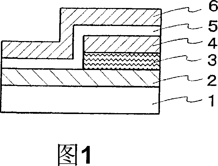
[0048] Next, the organic semiconductor element of the present invention and an organic EL display device using the organic semiconductor element will be described with reference to the drawings. The organic semiconductor element of the present invention, as shown in the cross-sectional explanatory diagram of one embodiment thereof in FIG. On the conductive layer 2, the organic semiconductor layer 3 and the second conductive layer 4 serving as the other of the source electrode and the drain electrode are provided. In the example shown in FIG. 1 , the organic semiconductor layer 3 and the second conductive layer 4 are formed smaller than the first conductive layer 2 and have a structure in which a part of the first conductive layer 2 is exposed. On its surface, there is a FET formed by providing a gate electrode (third conductive layer) 6 via an insulating layer 5 as a gate insulating film. In addition, the substrate 1 is very thick compared with other layers, and the relations...
PUM
 Abstract
Description
Claims
Application Information