
Organic el panel and method for manufacturing same

a technology of organic el panels and manufacturing methods, applied in the direction of thermoelectric device junction materials, electrical equipment, semiconductor devices, etc., can solve the problem of relatively low barrier to achieve the manufacturing of large organic el panels, and achieve excellent light-emitting characteristics and wide width

Active Publication Date: 2015-02-26
JOLED INC
View PDF2 Cites 14 Cited by
  • Summary
  • Abstract
  • Description
  • Claims
  • Application Information

AI Technical Summary

Benefits of technology

This patent describes an organic EL panel with good light-emitting properties. The panels have different colored organic layers, and banks are used to separate these layers. The banks with wider widths prevent ink of different colors from mixing and create well-formed organic layers. These technical features improve the quality and performance of the organic EL panels.

Problems solved by technology

Hence, the technical barrier to be overcome in realizing the manufacturing of large organic EL panels is relatively low.

Method used


Image

  • Organic el panel and method for manufacturing same
  • Organic el panel and method for manufacturing same
  • Organic el panel and method for manufacturing same

Examples


embodiment 1

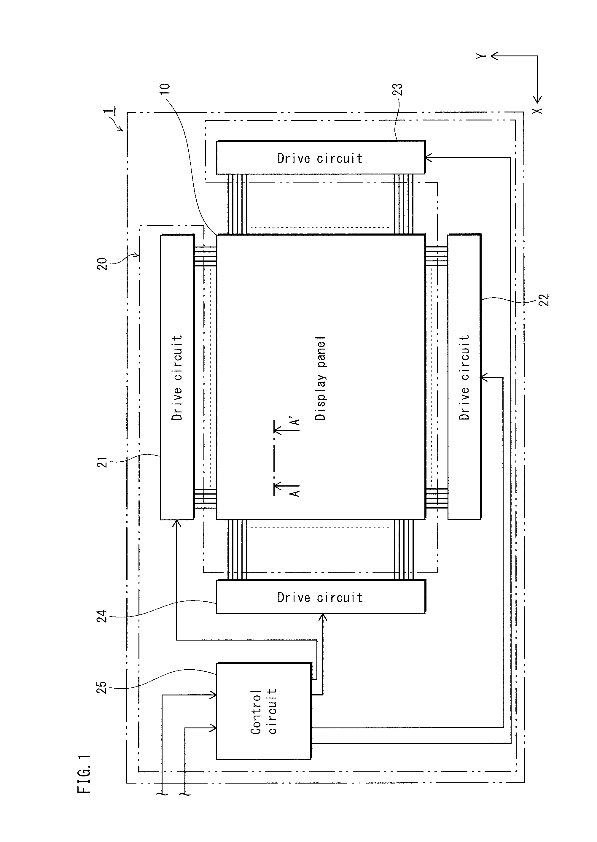
[0039]FIG. 1 is a block diagram illustrating an overall configuration of an organic EL apparatus 1 pertaining to Embodiment 1.

(Organic EL Apparatus 1)

[0040]The organic EL apparatus 1 includes a display panel 10 and a drive controller 20 connected thereto.

[0041]The display panel 10 is an organic EL panel having a plurality of organic EL elements aligned along the X direction and the Y direction intersecting with each other (at right angles in this example), and thus the organic EL elements are arranged in a matrix.

[0042]The drive controller 20 includes four drive circuits 21 through 24 and a control circuit 25, for example. The number of the drive circuits may be other than four.

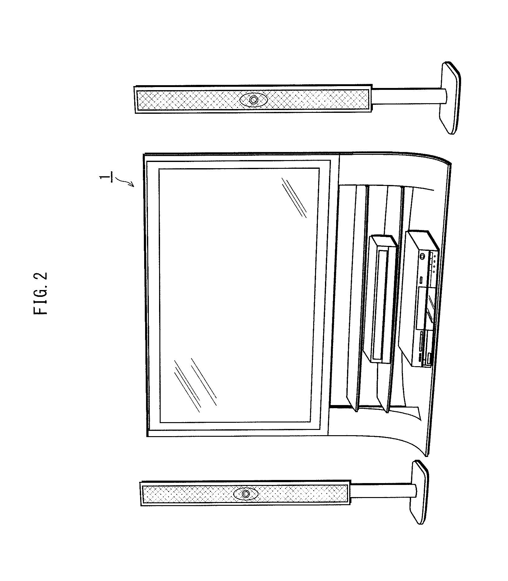
[0043]The organic EL apparatus 1 serves as, for example, a part of TV system, the appearance of which is as shown in FIG. 2. Unlike LCDs, the organic EL apparatus 1 can be thin because it does not require a backlight, and is advantageous in terms of system designing.

(Configuration of Display Panel 10)

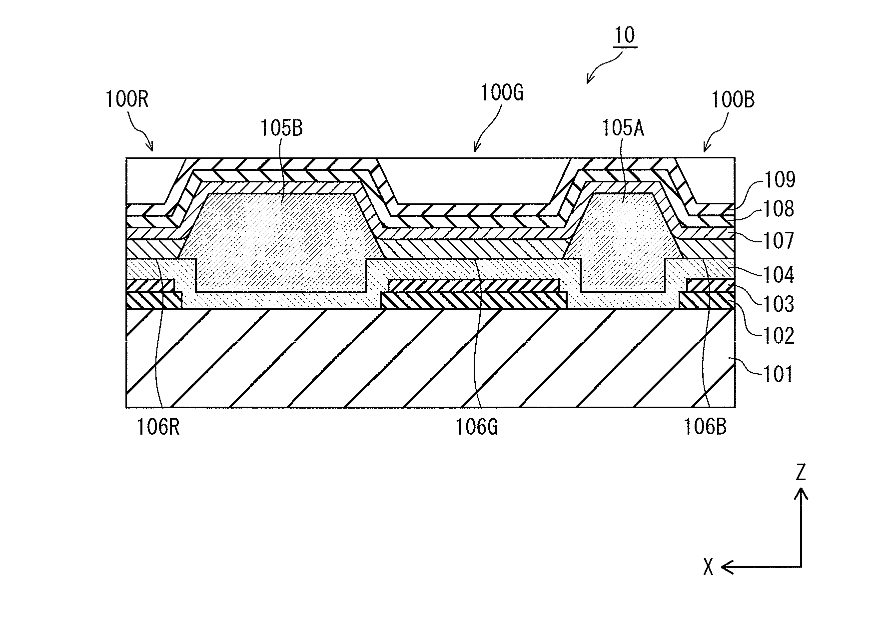
[0044]FI...

second embodiment

[0117]FIG. 10 is a panel frontal view showing the configuration of a display panel 30 pertaining to Embodiment 2.

[0118]The overall configuration of the display panel 30 is the same as the display panel 10. The difference is that pixel banks are provided to surround each of the elements 300R, 300G and 300B. The pixel banks include first banks (305B), second banks (305A) and third banks (305D). Among these, the banks 305B provided at both ends of the element 300R in the X direction are formed wider than the banks 305A and 305D. Although the widths of the banks 305A and 305D may be the same or different, it is preferable that they are smaller than the banks 305B in order to design all the banks with consideration of margins.

[0119]The display panel 30 with this configuration achieves almost the same advantageous effects as the display panel 10.

[0120]That is, during the manufacturing process, the stated configuration prevents color mixture at both ends of particularly the banks 305B in t...


PUM


Abstract

An organic EL panel including an organic light-emitting layer with a miniaturized structure formed by a wet process, allowing for excellent light-emitting characteristics, and a method for manufacturing the same. Specifically, the display panel includes: a substrate; first electrodes arranged above the substrate along a first and second direction intersecting with each other; a first, second, and third organic light-emitting layer arranged above the first electrodes so as to be adjacent to each other in the second direction, and each containing an organic light-emitting material corresponding to a different emission color; a first bank separating the first and the second layer; a second bank separating the second and the third layer; and a second electrode disposed above the first, the second, and the third layer and being different in polarity from the first electrodes. The first and the second bank are different in width along the second direction.

Description

TECHNICAL FIELD [0001]The present invention relates to an organic EL panel and a manufacturing method for the same, and in particular to a method for proper formation of an organic light-emitting layer by a wet process.BACKGROUND ART [0002]In recent years, progress has been made in research and development of diverse functional devices which involve use of an organic semiconductor.[0003]One typical example of such functional devices is an organic EL device. The organic EL element, which is a current-driven light-emitting element, includes a pair of electrodes, i.e. an anode and a cathode, and a functional layer layered between the pair of electrodes, the functional layer containing an organic material. The functional layer includes layers such as an organic light-emitting layer and a buffer layer. Further, there are cases where a hole injection layer is disposed between the functional layer and the anode. The hole injection layer is disposed for injecting holes to the functional lay...

Claims


Application Information

Patent Timeline
IPC IPC(8): H01L51/00H01L51/56H01L27/32
CPCH01L51/0004H01L51/56H01L27/3218H10K59/353H10K59/122H10K71/40H10K71/135H10K71/13H10K59/35H10K71/00
Inventor MATSUSHIMA, HIDEAKI
Owner JOLED INC
Learn More