Horizontal power LED device and method for manufacturing same

a technology of led devices and horizontal beams, which is applied in the direction of semiconductor/solid-state device manufacturing, semiconductor devices, electrical equipment, etc., can solve the problems of low yield, complicated processes, and non-uniform light emission of horizontal beams, and achieve high efficiency, reduce light emission areas, and high power

Active Publication Date: 2015-02-26
BAE JEONG WOON +2
View PDF1 Cites 8 Cited by
  • Summary
  • Abstract
  • Description
  • Claims
  • Application Information

AI Technical Summary

Benefits of technology

[0028]First, according to the horizontal power LED device and manufacturing method thereof, high power and high efficiency can be exhibited because the reduction of a light emission area caused by an electrode can be maximized.
[0029]Further, according to the horizontal power LED device and manufacturing method thereof, high power and high efficiency can be exhibited because the thickness of an n-clad layer can be maintained.
[0030]Further, according to the horizontal power LED device and manufacturing method thereof, high power and high efficiency can be exhibited because an N-electrode is formed on a Ga-face to provide low Vf.
[0031]Further, according to the horizontal power LED device and manufacturing method thereof, high power and high efficiency can be exhibited because the entire spreading is conducted by an embedded grid electrode, while current spreading is horizontally conducted, thus not causing a current crowding phenomenon.
[0032]Further, according to the horizontal power LED device and manufacturing method thereof, this horizontal power LED device has conventional vertical chip characteristics due to the formation of a metal substrate, has flip chip characteristics because a sub-mount or a soldering process is not required, and can exhibit high power and high efficiency because the improvement of efficiency of light extraction can be expected due to the formation of unevenness.

Problems solved by technology

Such a horizontal LED device has a low current spreading effect and a high current crowding effect, emits light non-uniformly, and has a small emitting area per chip.
Therefore, this horizontal LED device is disadvantageous for use in a large area.
However, this flip-chip LED device additionally requires a sub-mount and a soldering process.
However, this vertical LED device has a problem of complicated processes and a low yield.

Method used


Image

  • Horizontal power LED device and method for manufacturing same
  • Horizontal power LED device and method for manufacturing same
  • Horizontal power LED device and method for manufacturing same

Examples


Embodiment Construction

[0038]It will be further understood that terms, such as those defined in commonly used dictionaries, should be interpreted as having a meaning that is consistent with their meaning in the context of the relevant art and the present disclosure, and will not be interpreted in an idealized or overly formal sense unless expressly so defined herein.

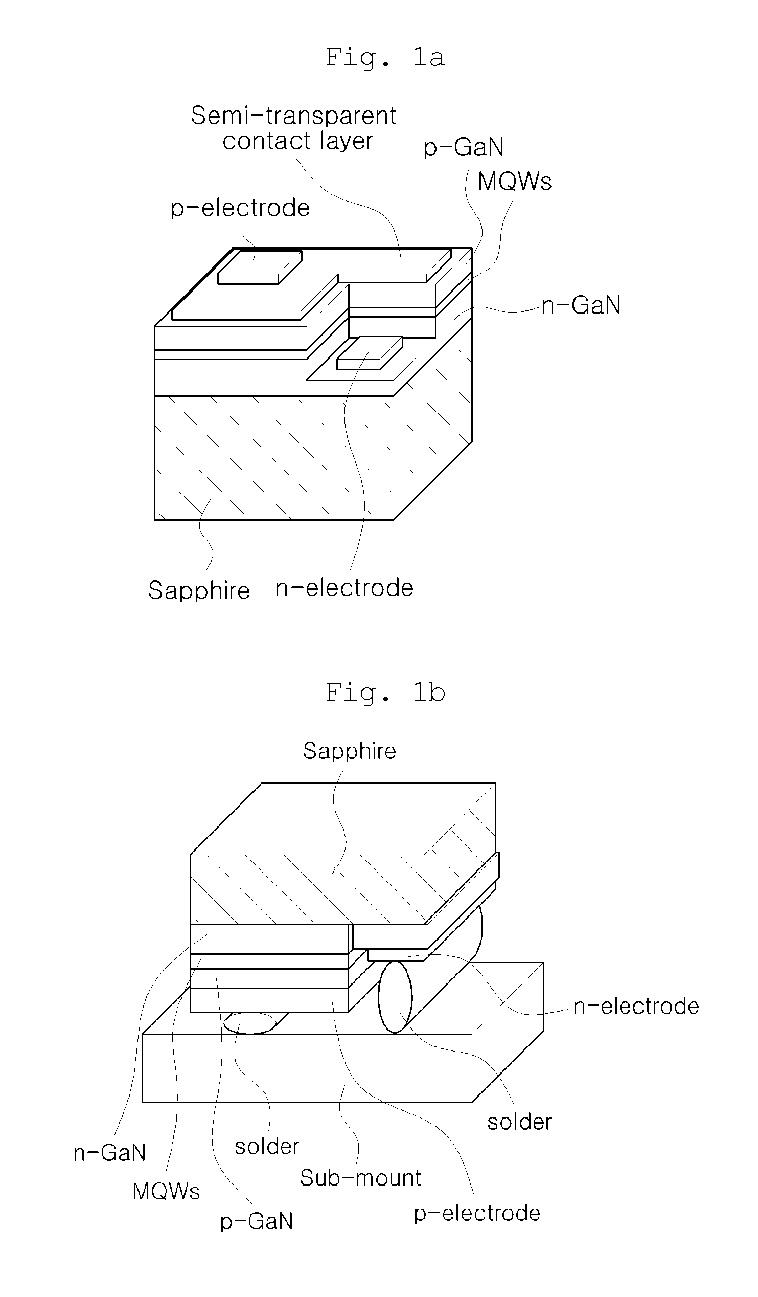
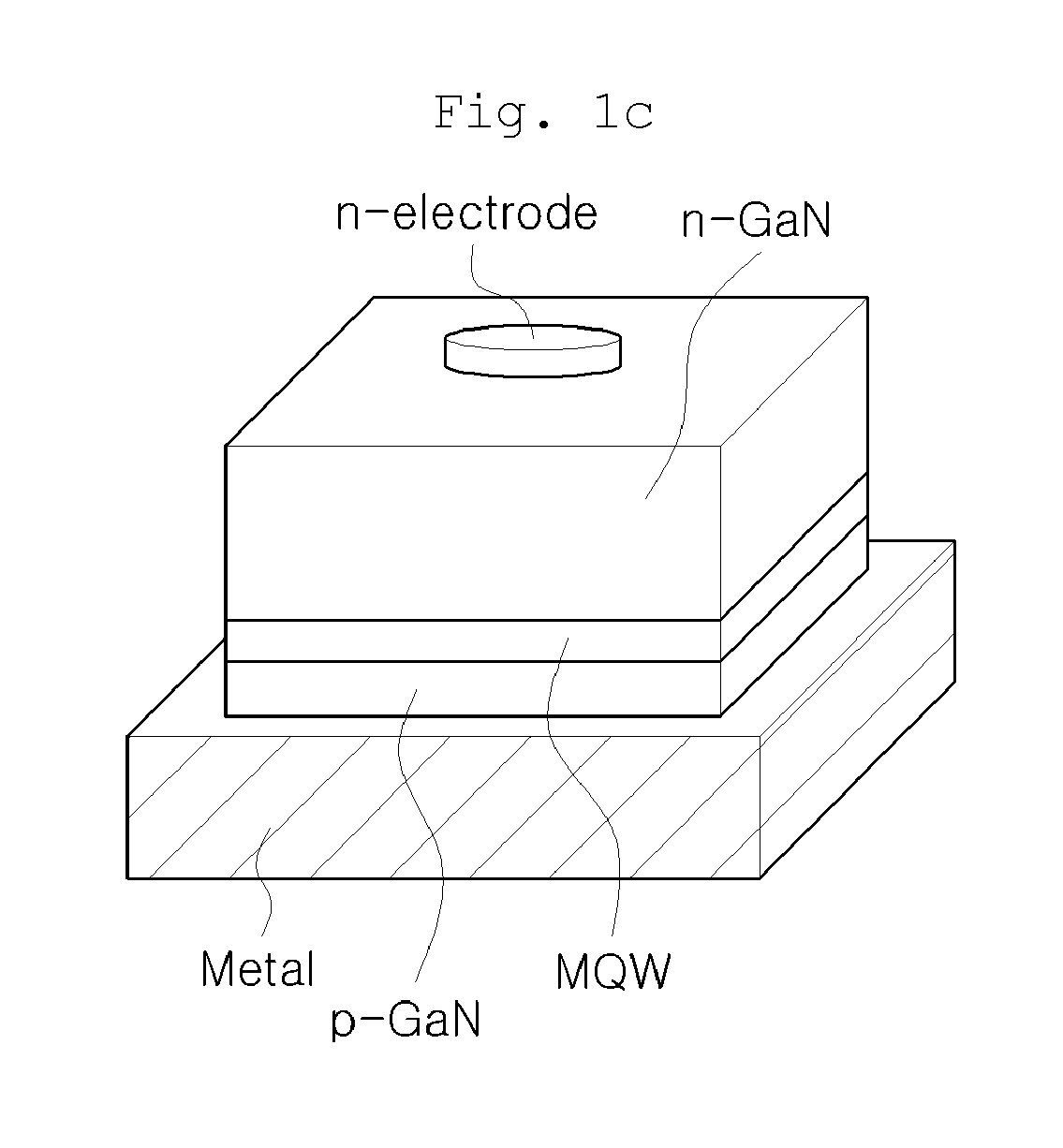
[0039]Hereinafter, preferred embodiments of the present invention will be described in detail with reference to the attached drawings.

[0040]Throughout the accompanying drawings, the same reference numerals are used to designate the same or similar components, and redundant descriptions thereof are omitted.

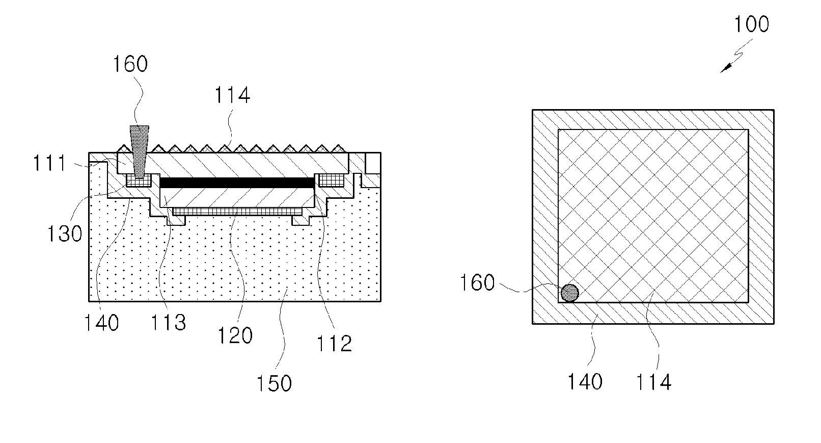
[0041]The horizontal power LED device and manufacturing method thereof according to the present invention is technically characterized in that the reduction of a light-emitting area attributable to electrodes can be minimized, the thickness of an n-clad layer can be maintained, an N-electrode can be formed on a conventional Ga-face, and a met...


PUM

PropertyMeasurementUnit
semiconductoraaaaaaaaaa
sizeaaaaaaaaaa
voltageaaaaaaaaaa

Abstract

The present invention relates to a horizontal LED device and a method of manufacturing the same. More particularly, the present invention relates to a high-power and high-efficiency horizontal LED device manufactured using the advantages of conventional horizontal and vertical LEDs, and a method of manufacturing the same.

Description

CROSS REFERENCE TO RELATED APPLICATIONS AND CLAIM OF PRIORITY[0001]This patent application is a National Phase application under 35 U.S.C. §371 of International Application No. PCT / KR2012 / 002089, filed Mar. 22, 2012, entire contents of which are incorporated herein by reference.BACKGROUND[0002]1. Technical Field[0003]The present invention relates to a horizontal LED device and a method of manufacturing the same. More particularly, the present invention relates to a high-power and high-efficiency horizontal LED device, which is manufactured by using the advantages of conventional horizontal and vertical LEDs, and a method of manufacturing the same.[0004]2. Background Art[0005]Generally, as shown in FIG. 1a, a horizontal LED device is configured in the basic form of a light-emitting structure including one light-emitting active layer (MQWS) and two cladding layers (p-GaN, n-GaN) covering both sides of the active layer. The cladding layers making contact with electrodes are n-doped and...

Claims


Application Information

Patent Timeline
Patent Type & Authority Applications(United States)
IPC IPC(8): H01L33/14H01L33/00H01L33/42H01L33/32H01L33/24
CPCH01L33/14H01L33/32H01L33/24H01L2933/0025H01L33/0075H01L2933/0016H01L33/42H01L33/382H01L33/0008H01L33/0095H01L2933/0033H01L2933/0066
Inventor BAE, JEONG WOONRYU, SEONG WOOKSHIM, JONG YOUNG
Owner BAE JEONG WOON
Why Eureka
Try Eureka