Local interconnects by metal-iii-v alloy wiring in semi-insulating iii-v substrates

a technology of metal-iiiv alloy wiring and semi-insulating iiiv, which is applied in the direction of semiconductor devices, semiconductor/solid-state device details, electrical apparatus, etc., can solve the problems of converting into a conductive material, and limiting the density of the device, so as to achieve the effect of interconnection formation

Inactive Publication Date: 2015-02-26
GLOBALFOUNDRIES INC
View PDF6 Cites 3 Cited by
  • Summary
  • Abstract
  • Description
  • Claims
  • Application Information

AI Technical Summary

Benefits of technology

[0007]In view of the foregoing, and other, exemplary problems, drawbacks, and disadvantages of the conventional systems, it is an exemplary feature of the present invention to provide a structure and method which allows the formation of interconnects on a semi-insulating semiconductor more efficiently.

Problems solved by technology

The BOX, however, consists of silicon dioxide (SiO2) which is an insulator, and cannot be transformed into a conductive material to form local wiring.
The process of connecting the above devices using conventional interconnects adds significant cost to the final device and may limit device density.

Method used


Image

  • Local interconnects by metal-iii-v alloy wiring in semi-insulating iii-v substrates
  • Local interconnects by metal-iii-v alloy wiring in semi-insulating iii-v substrates
  • Local interconnects by metal-iii-v alloy wiring in semi-insulating iii-v substrates

Examples


Embodiment Construction

[0020]Referring now to the drawings, and more particularly to FIGS. 1-8, there are shown exemplary embodiments of methods and structures according to the present invention.

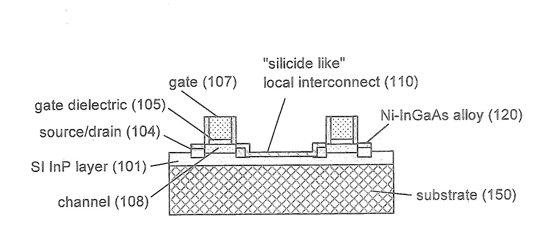
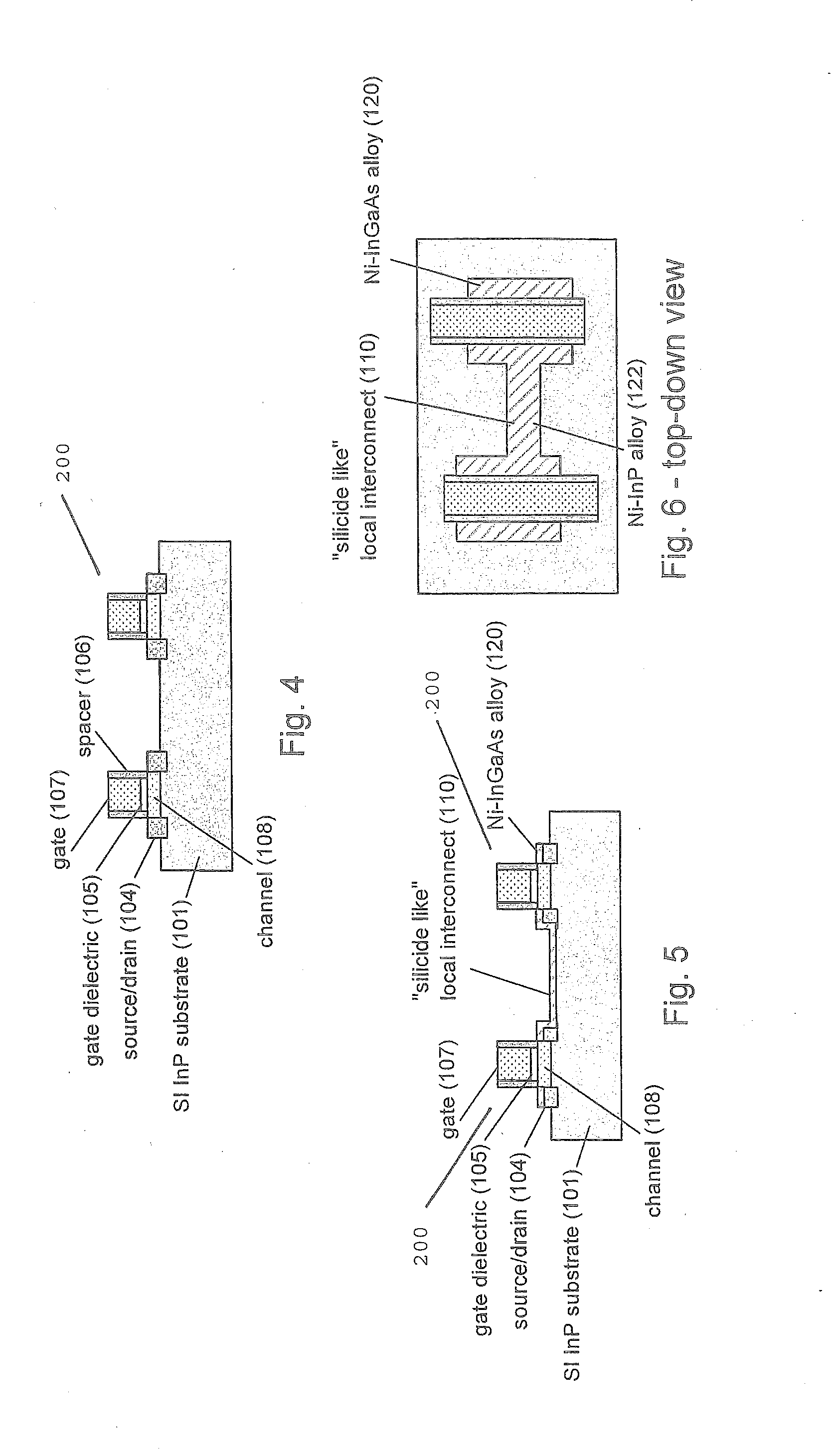
[0021]As noted above, the BOX in a SOI device is always an insulator and cannot be transformed into a conductive material to form local wiring. This is not the case when semi-insulating III-V substrates or layers are used.

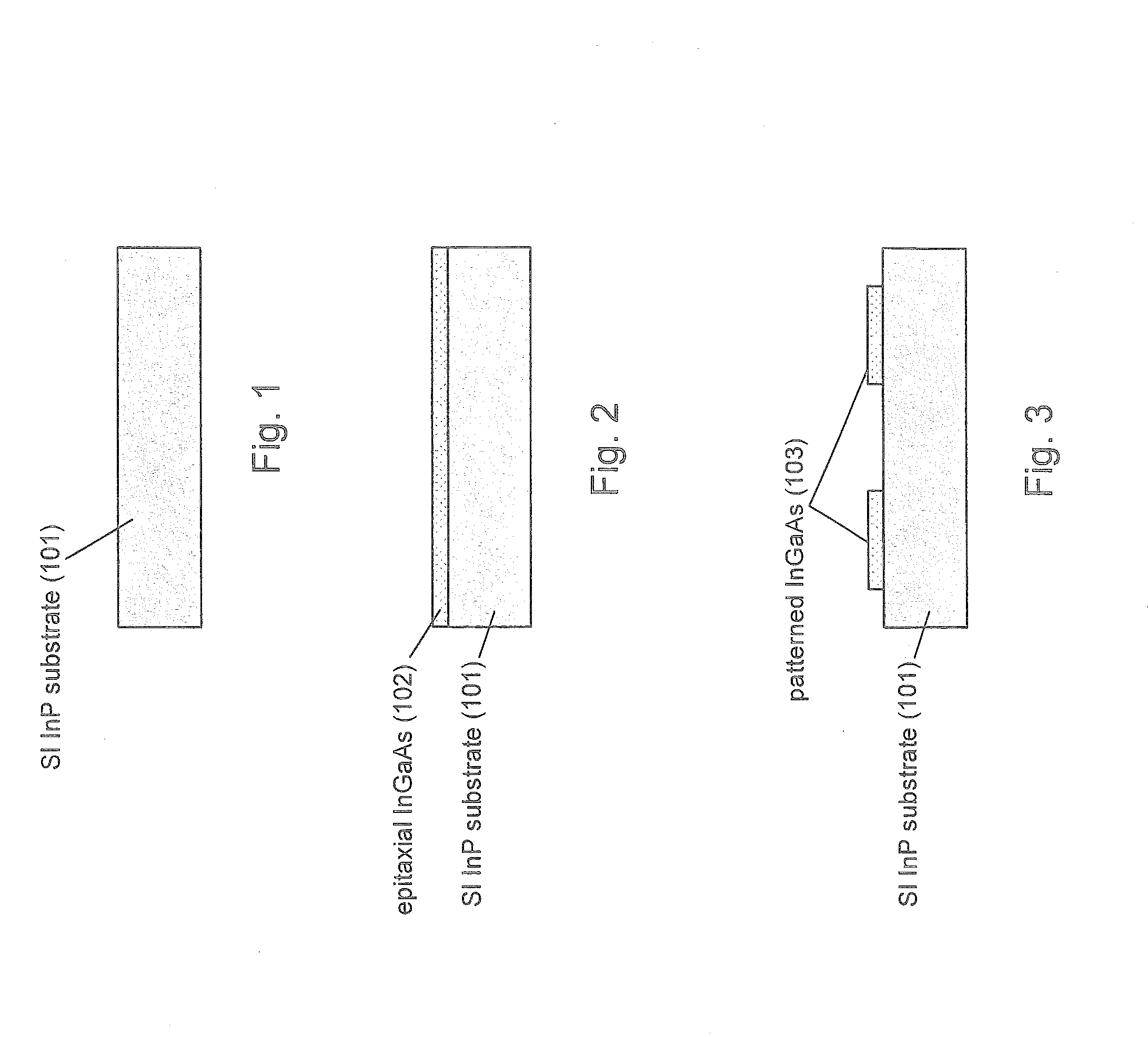
[0022]A semi-insulating (SI) material, for example SI InP, can be made conductive by reacting the InP with a metal such as Ni or Co. Thus, it is possible to make a conductive wire in SI InP by a process where Ni is reacted with InP to fowl a Ni—InP alloy. The material adjacent to the Ni—InP wire remains SI InP and is therefore non-conductive. An exemplary embodiment of the invention includes foaming of local interconnects between InGaAs devices by making Ni—InP wires in a SI InP.

[0023]Of course, the semi-insulating substrate can be made of other materials. For example, GaAs is turned into a semi ...


PUM

PropertyMeasurementUnit
temperatureaaaaaaaaaa
temperaturesaaaaaaaaaa

Abstract

A structure and method of producing a semiconductor structure including a semi-insulating semiconductor layer, a plurality of isolated devices formed over the semi-insulating semiconductor layer, and a metal-semiconductor alloy region formed in the semi-insulating semiconductor layer, where the metal-semiconductor alloy region electrically connects two or more of the isolated devices. The metal-semiconductor alloy region has a metal concentration in a range from 1×10²¹ atoms / cm3 to 1×10²³ atoms / cm3

Description

[0001]The present application is a Continuation-In-Part Application of U.S. patent application Ser. No. 13 / 905,894, filed on May 30, 2013, the entire content of which is incorporated herein by reference.DESCRIPTIONField of the Invention[0002]The present invention relates generally to a semi-insulating semiconductor layer having components formed thereon connected by a metal-semiconductor alloy.BACKGROUND OF THE INVENTIONDescription of the Related Art[0003]Devices fabricated using silicon on insulator (SOI) technology are isolated using a shallow trench isolation (STI) process or simply by etching the SOI film that would otherwise connect two active regions of separate devices. The device isolation (e.g. for planar or Fin Field-Effect Transistors (FETs)) is obtained by etching the SOI film down to the buried oxide (BOX). The BOX, however, consists of silicon dioxide (SiO2) which is an insulator, and cannot be transformed into a conductive material to form local wiring.[0004]Semi-insu...

Claims


Application Information

Patent Timeline
Patent Type & Authority Applications(United States)
IPC IPC(8): H01L27/088H01L29/201H01L29/205H01L23/532H01L21/24H01L21/768H01L29/207H01L29/06H01L29/20H01L21/8234
CPCH01L27/088H01L29/20H01L29/201H01L29/205H01L23/53209H01L21/24H01L21/768H01L29/207H01L29/0649H01L21/823475H01L21/76895H01L23/53271H01L2924/0002H01L2924/00
Inventor COHEN, GUYCABRAL, JR., CYRILBASU, ANIRBAN
Owner GLOBALFOUNDRIES INC
Why Eureka
Try Eureka