Method of etching silicon nitride film and method of producing semiconductor device

a silicon nitride film and etching technology, applied in the field of methods, can solve the problems of insufficient inability to achieve sufficient effect of etching method, and poor electrical conductivity of fluoride, and achieve the effect of suppressing the formation of copper fluorid

Inactive Publication Date: 2005-05-17
RENESAS ELECTRONICS CORP
View PDF18 Cites 2 Cited by
  • Summary
  • Abstract
  • Description
  • Claims
  • Application Information

AI Technical Summary

Benefits of technology

[0021]According to the present invention, it is made possible to effectively suppress the formation of copper fluorides that is difficult to remove, by using a mixture of fluorocarbon gas that contains

Problems solved by technology

While Al has been used predominantly as the metallic material to form interconnects, there has been a problem of electro-migration (EM) wherein a temperature rise due to the increasing current density through the interconnects and the heat generated from the entire device mobilizes metal atoms in the interconnects layer, thus eventually generating voids in the portion of migration, leading to interconnects breakage.
There is also such a problem that a block of grains referred to as “hillock” is formed in a portion where metal atoms are accumulated, which causes a stress in an insulation layer formed on the wiring, eventually causing cracks.
However, sufficient effect of this method cannot be achieved when the interconnects become finer and the packaging densit

Method used


Image

  • Method of etching silicon nitride film and method of producing semiconductor device
  • Method of etching silicon nitride film and method of producing semiconductor device
  • Method of etching silicon nitride film and method of producing semiconductor device

Examples


example 1

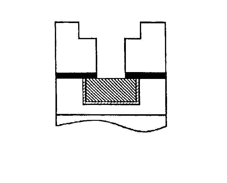
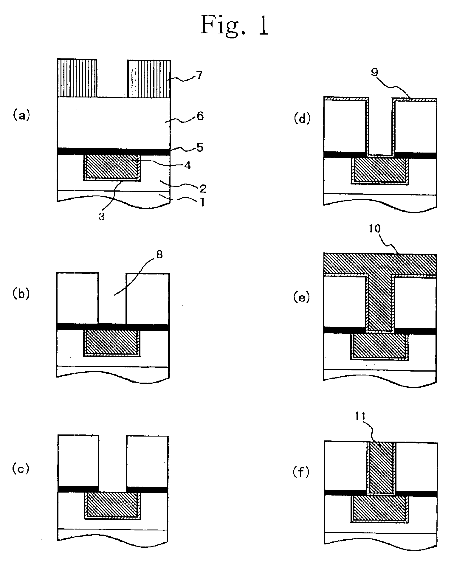
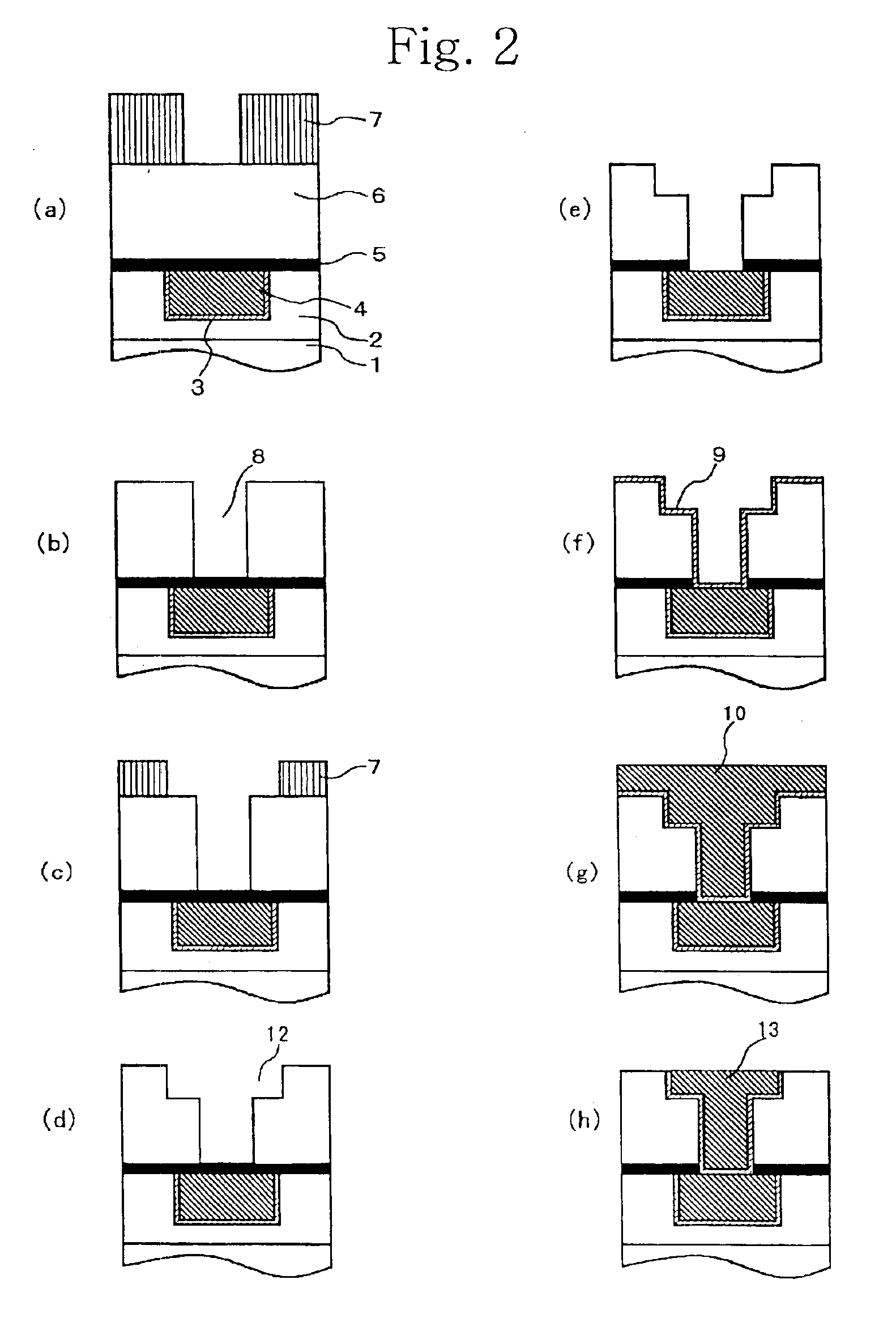
[0048]With reference to the drawing, description will now be made. FIG. 1 is a sectional view showing a process of the so-called single damascene forming method wherein copper is embedded in via holes formed in an inter-layer insulation film. First, as shown in FIG. 1(a), after forming functional elements such as transistors, that are not shown in the drawing, on a semiconductor substrate 1 such as silicon, a silicon oxide film is formed as an inter-layer insulation film 2. After forming interconnect grooves in the inter-layer insulation film 2, a barrier film 3 and a copper film are deposited therein and the surface is smoothed by the CMP polishing process, thereby forming an under-layer copper wiring 4 as a first wiring layer having thickness of 300 nm. A silicon nitride film that serves as an etching stopper film 5 having a thickness of 100 nm is formed on the under-layer copper interconnects 4 by the plasma CVD process, and a silicon nitride film having a thickness of 800 nm is ...

example 2

[0052]The copper plug was formed similarly to Example 1, except for modifying the conditions of removing the stopper film to contain oxygen of Experiment 5 and omitting the oxygen plasma processing after the etching. This resulted in less formation of copper fluoride and fluorocarbon deposit, showing that normal formation of the barrier film and embedding of the copper plugs are possible without applying the oxygen plasma processing.

[0053]Although the silicon oxide film (SiO2) is used as the inter-layer insulation film formed on the semiconductor substrate and on the silicon nitride film in the cases described above, the present invention is not limited to this constitution and any material known in the prior art, that allows the use of silicon nitride film as the etching stopper film, may be used. For example, BPSG (phospho-boro silicate glass), PSG (phospho-silicate glass), BSG (boro-silicate glass) and organic film having a low dielectric constant such as polyimide may be used. I...


PUM


Abstract

Provided is a method of etching a silicon nitride film, which comprises subjecting the silicon nitride film located on copper to dry etching using a mixture of fluorocarbon gas and an inert gas as the reaction gas, the fluorocarbon gas containing CF4 and CHF3 supplied at flow rates in a ratio of 3:7 to 0:1 or contains CF4 and CH2F2 supplied at flow rates in a ratio of 2.5:1 to 0:1, thereby suppressing the formation of copper fluoride.

Description

[0001]This application is a divisional Ser. No. of 09 / 739,891 filed on Dec. 20, 2000 now U.S. Pat. No. 6,613,686.BACKGROUND OF THE INVENTION[0002]1. Field of the Invention[0003]The present invention relates to a method of etching a silicon nitride film. The present invention also relates to a method of producing a semiconductor device and, more particularly, to a method that is effective in forming multilayer interconnects in a semiconductor device having copper interconnects.[0004]2. Description of the Related Art[0005]In recent years, in LSI devices that operate at increasingly higher speeds and are packaged at increasingly higher density, not only transistors but also conductive lines (interconnects) are required to be finer and formed at a higher density.[0006]While Al has been used predominantly as the metallic material to form interconnects, there has been a problem of electro-migration (EM) wherein a temperature rise due to the increasing current density through the interconn...

Claims


Application Information

Patent Timeline
IPC IPC(8): H01L21/02H01L21/311H01L21/302H01L21/3065
CPCH01L21/31116
Inventor NISHIZAWA, ATSUSHI
Owner RENESAS ELECTRONICS CORP
Why Eureka
Try Eureka