Display device
a display device and semiconductor technology, applied in semiconductor devices, instruments, electrical devices, etc., can solve the problems of reduced display quality of the display device, user perception of flickering images, etc., and achieve the effects of reducing wiring delay due to parasitic capacitance, excellent display quality, and low light leakag
- Summary
- Abstract
- Description
- Claims
- Application Information
AI Technical Summary
Benefits of technology
Problems solved by technology
Method used
Image

Examples
embodiment 1
[0073]In this embodiment, a display device which is one embodiment of the present invention is described with reference to drawings.
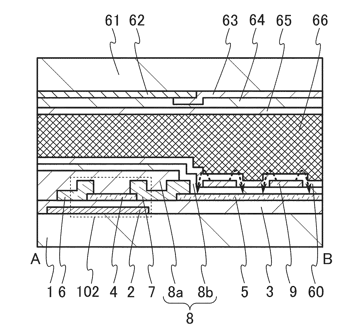
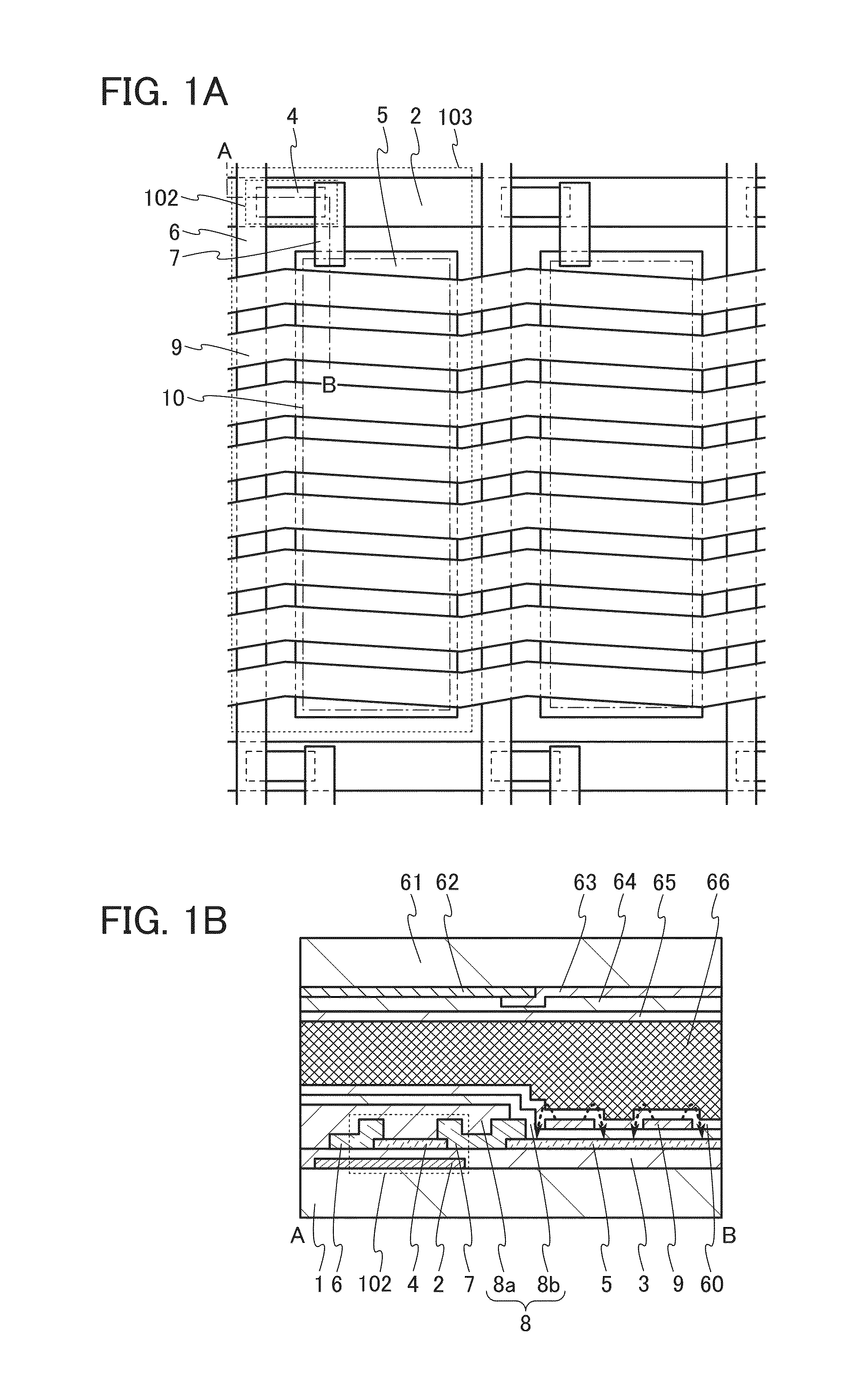
[0074]FIG. 1A is a top view of a pixel 103 of a display portion included in an FFS mode liquid crystal display device, and FIG. 1B is a cross-sectional view taken along dashed-dotted line A-B in FIG. 1A. In FIG. 1A, a substrate 1, an insulating film 3, an insulating film 8, an insulating film 60, a substrate 61, a light-blocking film 62, a coloring film 63, an insulating film 64, an insulating film 65, and a liquid crystal layer 66 are omitted.
[0075]As illustrated in FIGS. 1A and 1B, the FFS mode liquid crystal display device is an active matrix liquid crystal display device and includes a transistor 102 and a pixel electrode 5 in each pixel 103 provided in the display portion.
[0076]As illustrated in FIG. 1B, the liquid crystal display device includes the transistor 102 over the substrate 1, the pixel electrode 5 connected to the transistor 102, the ins...
modification example 2
[0137]In a common electrode 29 illustrated in FIG. 6, a first region and a second region are connected to each other. The first region has a stripe shape, is bent in a zigzag state, and intersects with an extending direction of a conductive film 21a functioning as a signal line. The second region is a region extending in a direction parallel or substantially parallel to the conductive film 21a functioning as a signal line. The common electrode 29 in FIG. 6 does not overlap with the conductive film 21a functioning as a signal line; therefore, parasitic capacitance of the common electrode 29 can be reduced.
[0138]However, the second region does not serve as a display region. Therefore, areas of the pixel 103a, the pixel 103b, and a pixel 103c get smaller, resulting in a low aperture ratio.
[0139]Thus, areas of a pixel 103d, a pixel 103e, and a pixel 103f can be increased by providing the second region connected to the first region over the conductive film 21a functioning as a signal lin...
embodiment 2
[0142]In this embodiment, a display device which is one embodiment of the present invention is described with reference to drawings. In addition, in this embodiment, an oxide semiconductor film is used as a semiconductor film included in a transistor.
[0143]A display device illustrated in FIG. 5A includes a pixel portion 101; a scan line driver circuit 104; a signal line driver circuit 106; m conductive films 107 functioning as scan lines which are arranged parallel or substantially parallel to each other and whose potentials are controlled by the scan line driver circuit 104; and n conductive films 109 functioning as signal lines which are arranged parallel or substantially parallel to each other and whose potentials are controlled by the signal line driver circuit 106. The pixel portion 101 further includes a plurality of pixels 103 arranged in a matrix. Furthermore, common lines 115 arranged parallel or substantially parallel to each other are provided along the conductive films 1...
PUM
 Abstract
Description
Claims
Application Information