Inverted metamorphic multijunction solar cells with doped alpha layer

a solar cell and metamorphic technology, applied in the field of inverted metamorphic multijunction solar cells with doped alpha layer, can solve the problems of presenting a number of practical difficulties and tending to be more complex in manufacture, and achieve the effect of increasing the photoconversion efficiency

Active Publication Date: 2015-04-02
SOLAERO TECH CORP
View PDF3 Cites 17 Cited by
  • Summary
  • Abstract
  • Description
  • Claims
  • Application Information

AI Technical Summary

Benefits of technology

[0044]It is an object of the present invention to provide increased photoconversion efficiency in a multijunction solar cell.
[0045]It is another object of the present invention to provide increased photoconversion efficiency in a multijunction solar cell by increasing the open circuit voltage of the overall solar cell.
[0047]It is another object of the present disclosure to decrease the statistical standard variation in the open circuit voltage from cell to cell as laid out across the surface of a single wafer as processed in an MOCVD reactor.
[0048]It is another object of the present invention to provide uniform and increased open circuit voltage or current in the multijunction solar cell(s) implemented on a single wafer as processed in an MOCVD reactor by utilizing a selenium or tellurium dopant during deposition of a grading metamorphic buffer layer.
[0049]It is another object of the present invention to provide uniform and increased open circuit voltage or current in inverted metamorphic multijunction solar cell(s) implemented on a single wafer as processed in an MOCVD reactor by utilizing a selenium or tellurium dopant during deposition of one or more layers adjacent to the grading metamorphic buffer layer.
[0072]In some embodiments, a second alpha layer is provided over said second solar subcell using a surfactant and dopant including selenium, the second alpha layer also configured to prevent threading dislocations from propagating.

Problems solved by technology

Compared to silicon, III-V compound semiconductor multijunction devices have greater energy conversion efficiencies and generally more radiation resistance, although they tend to be more complex to manufacture.
However, the materials and structures for a number of different layers of the cell proposed and described in such reference present a number of practical difficulties, particularly relating to the most appropriate choice of materials and fabrication steps.

Method used


Image

  • Inverted metamorphic multijunction solar cells with doped alpha layer
  • Inverted metamorphic multijunction solar cells with doped alpha layer
  • Inverted metamorphic multijunction solar cells with doped alpha layer

Examples


Embodiment Construction

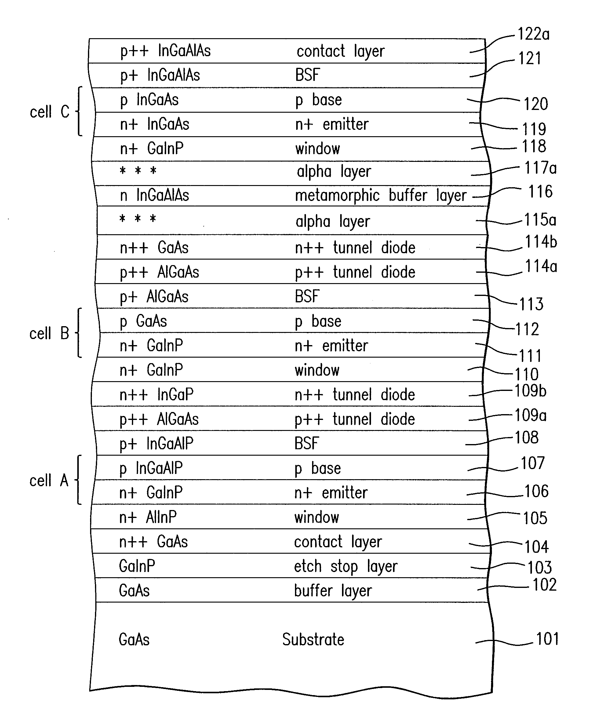
[0123]Details of the present invention will now be described including exemplary aspects and embodiments thereof. Referring to the drawings and the following description, like reference numbers are used to identify like or functionally similar elements, and are intended to illustrate major features of exemplary embodiments in a highly simplified diagrammatic manner. Moreover, the drawings are not intended to depict every feature of the actual embodiment nor the relative dimensions of the depicted elements, and are not drawn to scale.

[0124]The basic concept of fabricating an inverted metamorphic multijunction (IMM) solar cell is to grow the subcells of the solar cell on a substrate in a “reverse” sequence. That is, the high band gap subcells (i.e. subcells with band gaps in the range of 1.8 to 2.1 eV), which would normally be the “top” subcells facing the solar radiation, are initially grown epitaxially directly on a semiconductor growth substrate, such as for example GaAs or Ge, and...


PUM


Abstract

A method of forming a multijunction solar cell comprising at least an upper subcell, a middle subcell, and a lower subcell, the method including forming a first alpha layer over said middle solar subcell using a surfactant and dopant including selenium, the first alpha layer configured to prevent threading dislocations from propagating; forming a metamorphic grading interlayer over and directly adjacent to said first alpha layer; forming a second alpha layer using a surfactant and dopant including selenium over and directly adjacent to said grading interlayer to prevent threading dislocations from propagating; and forming a lower solar subcell over said grading interlayer such that said lower solar subcell is lattice mismatched with respect to said middle solar subcell.

Description

REFERENCE TO RELATED APPLICATIONS[0001]This application is related to co-pending U.S. patent application Ser. No. 14 / 026,818 filed Sep. 13, 2013.[0002]This application is related to co-pending U.S. patent application Ser. No. 13 / 954,610 and Ser. No. 13 / 954,630 filed Jul. 30, 2013.[0003]This application is related to co-pending U.S. patent application Ser. No. 13 / 921,756 filed Jun. 19, 2013.[0004]This application is related to co-pending U.S. patent application Ser. No. 13 / 836,742 filed Mar. 15, 2013.[0005]This application is related to co-pending U.S. patent application Ser. No. 13 / 831,406 filed Mar. 14, 2013.[0006]This application is related to co-pending U.S. patent application Ser. No. 13 / 768,683 filed Feb. 13, 2013.[0007]This application is related to U.S. patent application Ser. No. 12 / 637,241, filed Dec. 14, 2009, which is a continuation-in-part of U.S. patent application Ser. No. 11 / 616,596, filed Dec. 27, 2006, and Ser. No. 12 / 544,001, filed Aug. 19, 2009.[0008]This applicat...

Claims


Application Information

Patent Timeline
Patent Type & Authority Applications(United States)
IPC IPC(8): H01L31/0687H01L31/18
CPCH01L31/06875H01L31/184H01L31/1844H01L31/078Y02E10/544Y02P70/50H01L31/0336H01L31/065
Inventor CHO, BENJAMINLIN, YONGPATEL, PRAVINSTAN, MARK A.CORNFELD, ARTHURMCGLYNN, DANIELNEWMAN, FRED
Owner SOLAERO TECH CORP
Why Eureka
Try Eureka