Liquid crystal display device and method for manufacturing the same

a liquid crystal display and display device technology, applied in semiconductor devices, optics, instruments, etc., can solve the problems of low productivity of manufacturing liquid crystal displays, low yield, and inability to provide good viewing angle characteristics, so as to shorten the takt time and increase productivity.

Active Publication Date: 2015-04-02
LG DISPLAY CO LTD
View PDF5 Cites 18 Cited by
  • Summary
  • Abstract
  • Description
  • Claims
  • Application Information

AI Technical Summary

Benefits of technology

[0013]An object of the present invention is to provide a method for manufacturing a liquid crystal display which can shorten the takt time and increase productivity by reducing the number of masks used to manufacture the liquid crystal display.

Problems solved by technology

However, the driving of liquid crystal with the vertically applied electric field is disadvantageous in that it does not provide for good viewing angle characteristics.
With the use of a total of seven masks, the above-described related art method for manufacturing a liquid crystal display has a problem of low productivity because of the higher manufacturing costs and longer takt times associated with a relative high number of masks.
Also, the high number of mask processes may lead to a higher percentage of manufacturing defects, thus potentially resulting in a lower yield, a higher manufacturing cost, and a decrease in the performance of the finished products.

Method used


Image

  • Liquid crystal display device and method for manufacturing the same
  • Liquid crystal display device and method for manufacturing the same
  • Liquid crystal display device and method for manufacturing the same

Examples


Embodiment Construction

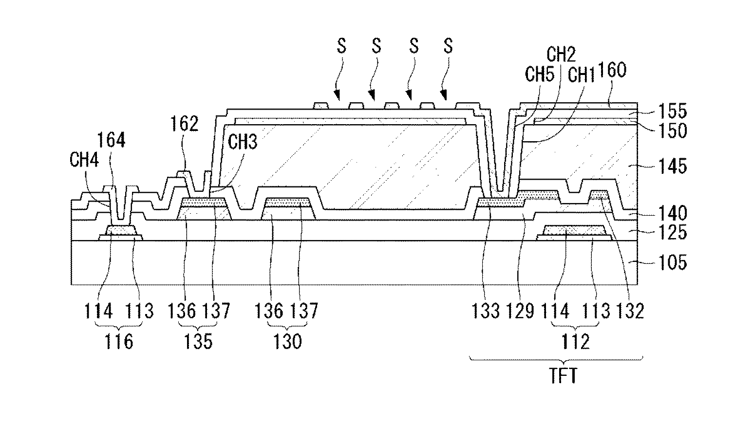
[0026]Reference will now be made in detail to embodiments of the present invention, examples of which are illustrated in the accompanying drawings. Wherever possible, the same reference numbers will be used throughout the drawings to refer to the same or like parts. Detailed description of known art may be omitted if the art can mislead the embodiments of the invention.

[0027]FIG. 2 is a top plan view showing an in-plane switching liquid crystal display according to one example embodiment of the present invention. FIG. 3 is a cross-sectional view showing an in-plane switching liquid crystal display according to one example embodiment of the present invention.

[0028]As shown in FIG. 2, the in-plane switching liquid crystal display according to the example embodiment of the present invention comprises a gate line 110 arranged in one direction on a substrate (not shown), a common line 120 arranged in parallel with and adjacent to the gate line 110, and a data line 130 crossing the gate l...


PUM

PropertyMeasurementUnit
widthaaaaaaaaaa
transparentaaaaaaaaaa
organicaaaaaaaaaa

Abstract

A disclosed liquid crystal display includes a substrate with a gate electrode, a gate insulation film, an active layer, a source electrode, a drain electrode, and a first passivation film formed on the substrate. An organic insulation film having a first contact hole and a common electrode having a second contact hole are formed on the first passivation film using a single mask. The display also includes a second passivation film on the common electrode, and a pixel electrode on the second passivation film and connected to the drain electrode via the contact hole through the second passivation film. The top surface of the organic insulation film adjacent to a side edge of the organic insulation film is uncovered by the common electrode.

Description

[0001]This application claims the priority benefit of Korean Patent Application No. 10-2013-0116006 filed in Korea on Sep. 30, 2013, which is incorporated by reference for all purposes as if fully set forth herein.BACKGROUND OF THE INVENTION[0002]1. Field of the Invention[0003]The present invention relates to a liquid crystal display and a method for manufacturing the same, and more particularly, to an in-plane switching liquid crystal display and a method for manufacturing the same which can shorten takt time and increase productivity by reducing the number of masks.[0004]2. Discussion of the Related Art[0005]A liquid crystal display is generally driven using optical anisotropy and polarization properties of liquid crystals. Because the liquid crystals have an elongated shape, liquid crystal molecules have an alignment orientation. The alignment orientation of the liquid crystal molecules may be controlled by applying an electric field to the liquid crystals. Thus, when the alignme...

Claims


Application Information

Patent Timeline
Patent Type & Authority Applications(United States)
IPC IPC(8): G02F1/1368G02F1/1362
CPCG02F1/1368G02F1/136227G02F1/136286G02F1/136295G02F1/134363G02F1/134372G02F1/13439H01L27/1248H01L27/1288
Inventor KIM, MINJOONOH, SOYOUNGKIM, YONGILKIM, TAEHWAN
Owner LG DISPLAY CO LTD
Why Eureka
Try Eureka