Processing apparatus, method for detecting ACF sticking state or display substrate assembly line

A technology for displaying substrates and assembly lines, applied in measuring devices, nonlinear optics, optics, etc., can solve problems such as device width growth, and achieve the effects of short assembly line length, shortened processing width, and shortened takt time

Inactive Publication Date: 2010-09-29
HITACHI HIGH-TECH CORP
View PDF3 Cites 10 Cited by
  • Summary
  • Abstract
  • Description
  • Claims
  • Application Information

AI Technical Summary

Problems solved by technology

[0005] Therefore, this results in a plurality of processing work parts before the final processing work part, and the pasting work is not performed, but only inspection time is required.
In addition, the head of the ACF pasting device needs to exceed (overrun) the multiple working parts, and the width of the device increases accordingly

Method used


Image

  • Processing apparatus, method for detecting ACF sticking state or display substrate assembly line
  • Processing apparatus, method for detecting ACF sticking state or display substrate assembly line
  • Processing apparatus, method for detecting ACF sticking state or display substrate assembly line

Examples


no. 1 approach

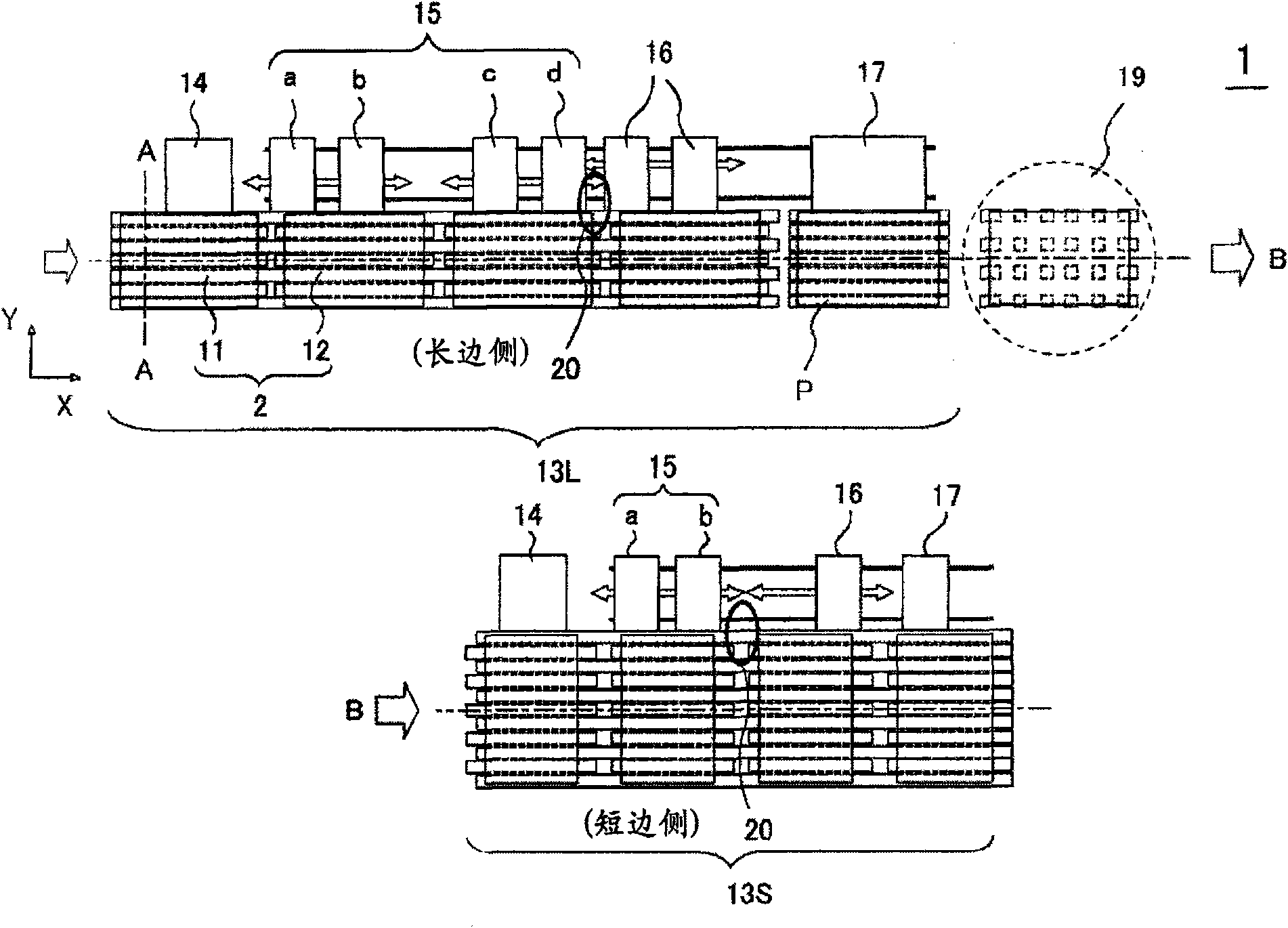
[0034] figure 1 A display substrate module assembly line 1 showing one embodiment of the present invention, figure 2 The basic structure of this substrate transfer device 2 is shown.

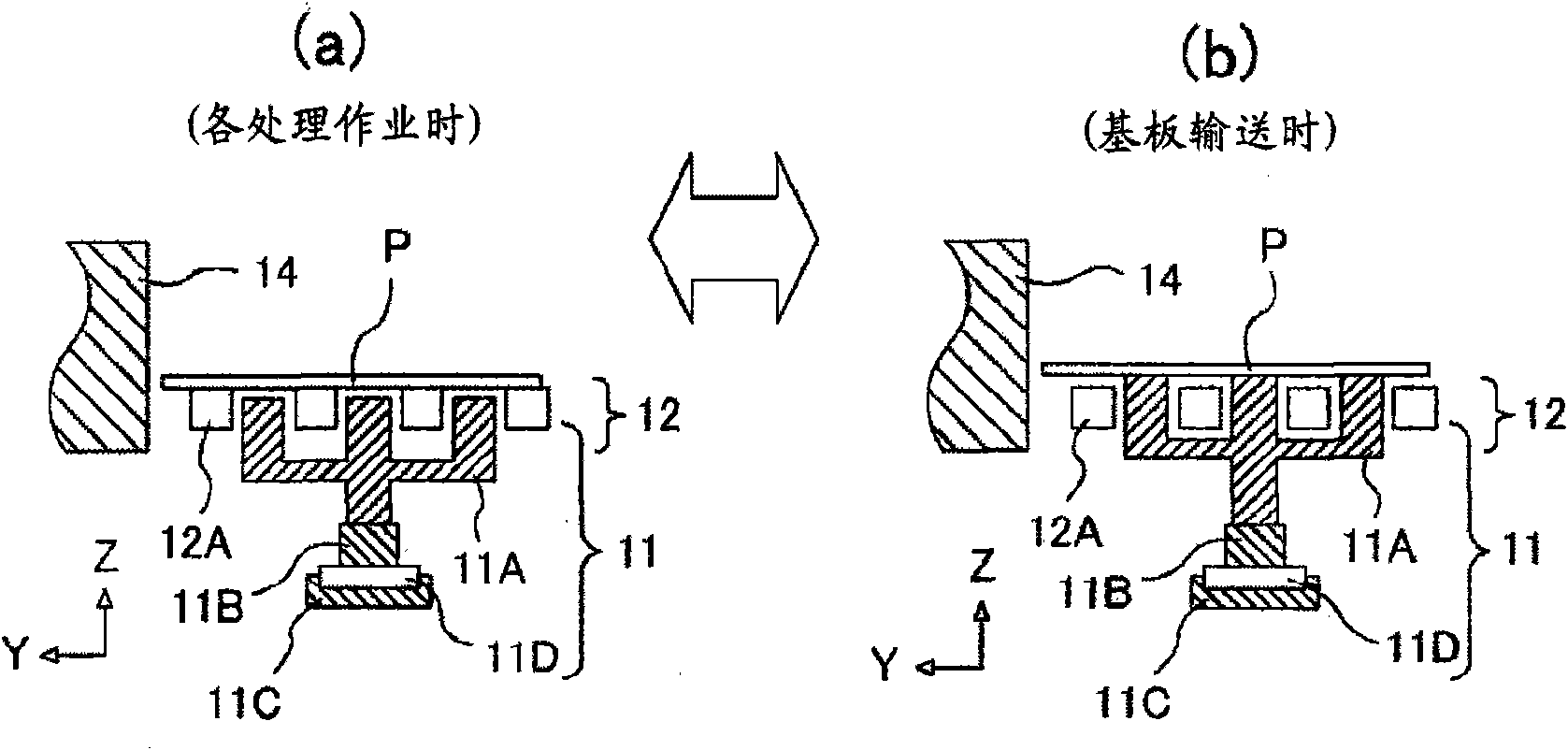
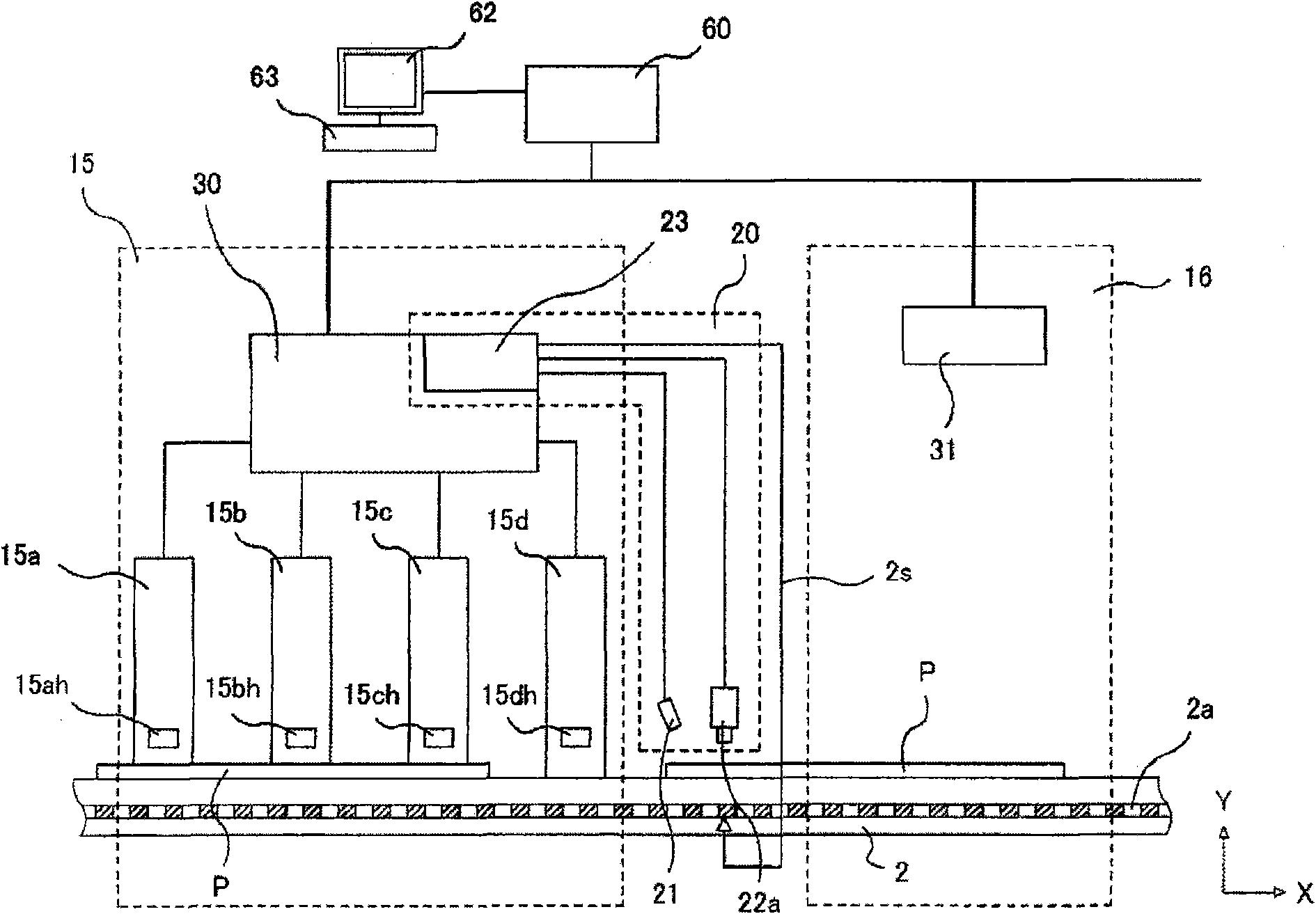
[0035] figure 1 is a device that is viewed from the left side in the figure by a conveying device composed of a substrate holding unit 12 holding a substrate P and a substrate conveying unit 11 for conveying the substrate to the position of an adjacent processing operation device. On the right side, substrates are conveyed sequentially, and at the same time, various processing operations are performed on the periphery of the substrates, and mounting and assembly operations such as ICs and TABs are performed. figure 1, firstly, the substrate long side is processed by the processing unit group 13L on the left side of the substrate long side, and after the substrate long side is processed, the substrate is rotated by the substrate rotation unit 19. The processing operation device group 13S on t...


PUM


Abstract

The invention provides a processing apparatus or a method for inspecting the ACF sticking state, capable of shortening the total time for the ACF sticking operation and the inspection operation of the ACF sticking state or shortening the width of the processing apparatus in the ACF sticking process, or a display substrate module assembly line, capable of shortening the beat time of the display substrate= module assemble or having short assembly line length. An ACF stuck at the predetermined positon of a display substrate is lighted and shot, when the ACF sticking state is inspected according to the shot result, the shooting and inspection are performed in the process of conveying the display substrate after the ACF is stuck.

Description

technical field [0001] The present invention relates to assembling driver ICs around display substrates of FPD (Flat Panel Display) such as liquid crystals or plasmas, or connecting so-called TAB (Tape Automated Bonding) such as COF (Chip on Film) and FPC (Flexible Printed Circuits), and mounting peripheral substrates (PCB=printed circuit board) processing equipment and display substrate module assembly line composed of them. More specifically, it relates to an inspection mechanism and an inspection method for inspecting the bonding state of an anisotropic conductive film (ACF=Anisotropic Conductive Film), and a display substrate module assembly line configured based on the inspection mechanism or inspection results. Background technique [0002] The display substrate module assembly line is to sequentially perform multiple processing operations on the display substrate of FPD such as liquid crystal and plasma (hereinafter referred to as the substrate, and in the case of oth...

Claims


Application Information

Patent Timeline
Patent Type & Authority Applications(China)
IPC IPC(8): G02F1/13G01N21/956
Inventor 海老泽圭一秋叶佑司比佐隆文武田正臣玉本淳一片保秀明土井秀明斋藤佳大
Owner HITACHI HIGH-TECH CORP
Why Eureka
Try Eureka