Light-emitting device and electronic apparatus

a technology of light-emitting devices and electronic devices, which is applied in the field of light-emitting devices, can solve the problems of insufficient connection between the second electrode and the peripheral wiring, and the height difference of a height, and achieve the effect of reducing the height difference of a second electrod

Active Publication Date: 2015-04-16
SEIKO EPSON CORP
View PDF1 Cites 21 Cited by
  • Summary
  • Abstract
  • Description
  • Claims
  • Application Information

AI Technical Summary

Benefits of technology

[0007]An advantage of some aspects of the invention is that a height difference that occurs in a second electrode is reduced. In addition, an advantage of some aspects of the invention is that conduction between electrodes of light-emitting elements and peripheral wirings is sufficiently achieved.

Problems solved by technology

Therefore, there is a problem in that there is a height difference of a height corresponding to the sum of the film thicknesses of the wiring side insulating layer and the electrode side insulating layer, between the surface of a region of the second electrode positioned outside the conduction hole in the plan view and the surface of a region thereof that penetrates into the conduction hole.
Accordingly, there is a problem in that the connection between the second electrode and the peripheral wiring becomes insufficient.

Method used


Image

  • Light-emitting device and electronic apparatus
  • Light-emitting device and electronic apparatus
  • Light-emitting device and electronic apparatus

Examples


first embodiment

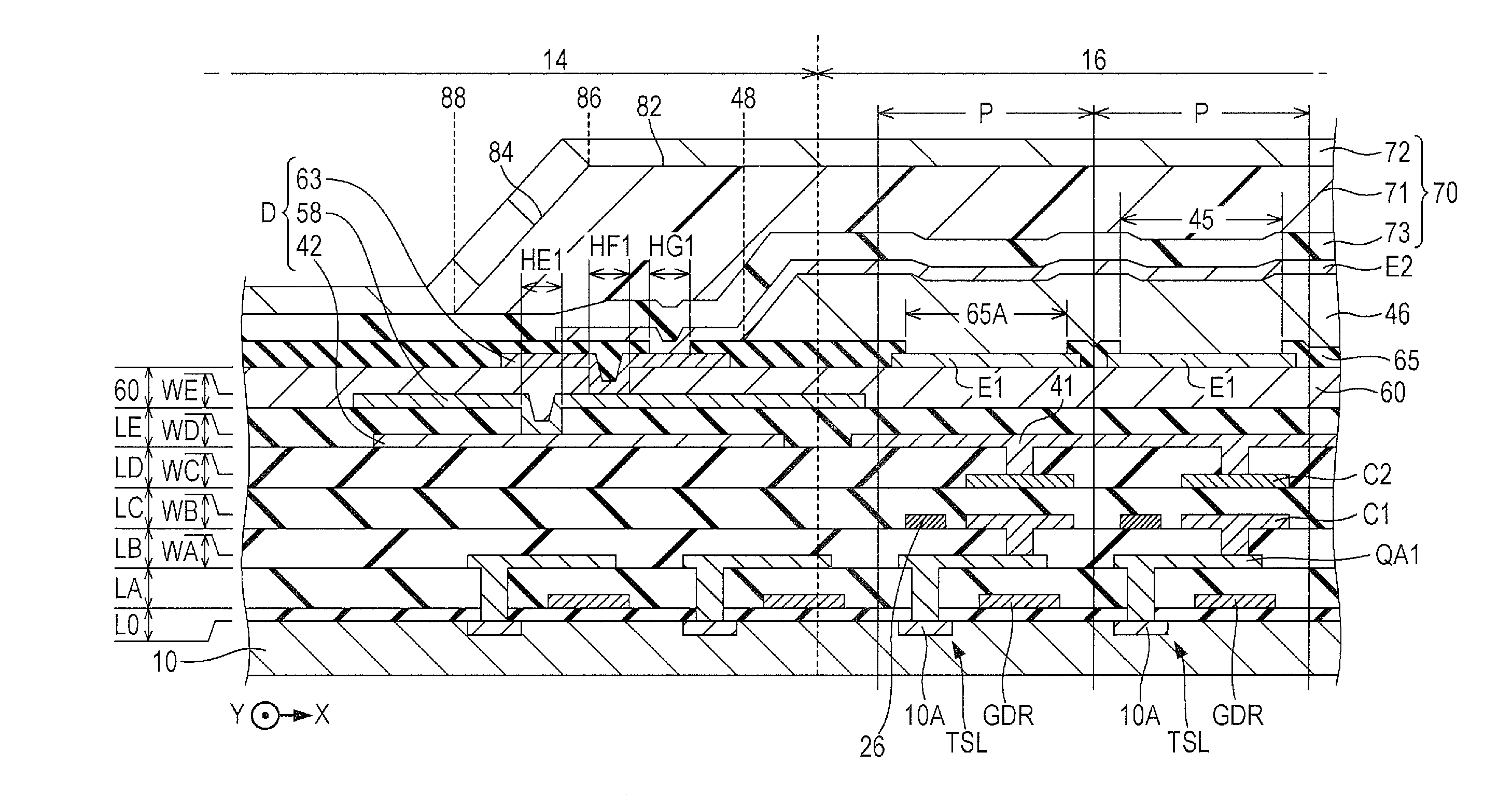
[0049]FIG. 1 is a plan view of a light-emitting device 100 according to a first embodiment of the invention. The light-emitting device 100 of the first embodiment is an organic EL device in which light-emitting elements that use an organic EL material are formed on the surface of a substrate 10. The substrate 10 is a plate-like member (semiconductor substrate) formed of a semiconductor material such as silicon and is used as a base body (base) on which a plurality of light-emitting elements are formed.

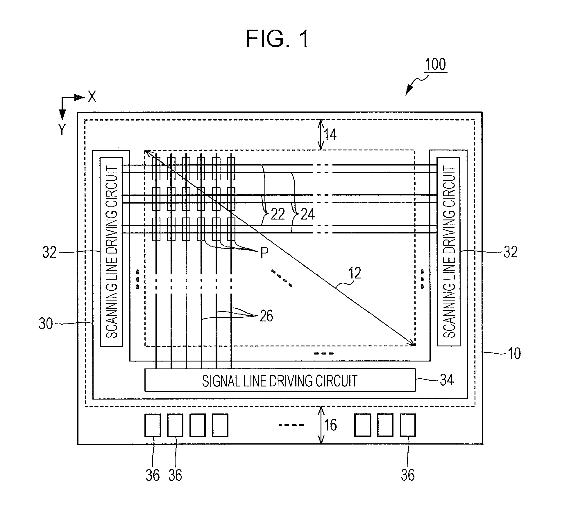
[0050]As exemplified in FIG. 1, a display region 12, a peripheral region 14, and a mounting region 16 are demarcated on the surface of the substrate 10. The display region 12 is a rectangular region in which a plurality of pixels P are arranged. In the display region 12, a plurality of scanning lines 22 that extend in an X direction, a plurality of control lines 24 that extend in the X direction to respectively correspond to the scanning lines 22, and a plurality of signal lines 26 tha...

second embodiment

[0108]A second embodiment of the invention will be described. In the embodiments exemplified as follows, like elements having the same actions or functions as those of the first embodiment are denoted by like reference numerals referred to in the description of the first embodiment, and detailed description thereof will be appropriately omitted.

[0109]FIG. 19 is an explanatory view of the filter layer 90 formed on the surface of the sealing body 70 of the second embodiment. As exemplified in FIG. 19, in the insulating layer 92 of the second embodiment, the opening 92B described in the first embodiment is not formed. The protection portion 96 of the second embodiment is different from that of the first embodiment in the positional relationship between the peripheral edges of the layers (the first, second, and third layers 96R, 96G, and 96B). In the first embodiment, the peripheral edges of the layers of the protection portion 96 overlap each other in the plan view (the side surfaces o...

modification example

[0112]The embodiments exemplified above may be modified in various forms. Specific modifications are exemplified as follows. Two or more forms that are arbitrarily selected from the following examples may be appropriately combined.

[0113](1) From the viewpoint of reducing the height difference in the surface of the filter layer 90, as illustrated in FIG. 20, the protection portion 96 having the same film thickness as that of the insulating layer 92 may be formed on the inside of the opening 92B formed in the insulating layer 92. According to the above configuration, as illustrated in FIG. 20, since the surface of the insulating layer 92 and the surface of the protection portion 96 are positioned on substantially the same plane, an effect of a reduction in the height difference in the surface of the filter layer 90 becomes more significant.

[0114]However, in the case where the spin coating method is employed to form the adhesive layer 21, there is a possibility that the adhesive that i...


PUM


Abstract

A light-emitting device includes: a light-emitting element which is disposed in a display region of a base body and includes a first electrode, a second electrode, and a light-emitting functional layer; a first conductor; a first insulating layer which covers the first conductor; a second conductor; and a second insulating layer which covers the second conductor. The second electrode is formed on a surface of the first insulating layer and is electrically connected to the first conductor via a first conduction hole of the first insulating layer, the first conductor is formed on a surface of the second insulating layer and is electrically connected to the second conductor via a second conduction hole of the second insulating layer, and the first conduction hole and the second conduction hole are configured not to overlap each other in a plan view.

Description

BACKGROUND[0001]1. Technical Field[0002]The present invention relates to a light-emitting device which uses a light-emitting material such as an organic electroluminescent (EL) material.[0003]2. Related Art[0004]A light-emitting device having light-emitting elements which use an organic EL material and are arranged on a display region of a substrate is hitherto suggested. The light-emitting element includes a first electrode (anode), a second electrode (cathode), and a light-emitting functional layer which emits light according to current between the two electrodes. A potential corresponding to the luminance for light emission is supplied to the first electrode, and a lower power supply potential is supplied to the second electrode. In JP-A-2001-109395 and JP-A-2013-54863, a light-emitting device in which a power supply wiring which is connected to the second electrode of the light-emitting element and supplies the power supply potential is formed in the periphery of the display reg...

Claims


Application Information

Patent Timeline
Patent Type & Authority Applications(United States)
IPC IPC(8): H01L27/32
CPCH01L27/3272H01L27/3276H10K59/1315H10K59/126H10K59/131
Inventor KOSHIHARA, TAKESHIOTA, HITOSHINOZAWA, RYOICHI
Owner SEIKO EPSON CORP
Why Eureka
Try Eureka