Current-perpendicular-to-the-plane (CPP) magnetoresistive (MR) sensor having an antiparallel free (APF) structure with improved magnetic stability
a technology of magnetic stabilization and applied in the field of current perpendicular to the plane (cpp) magnetoresistive (mr) sensor with an antiparallel free (apf) structure, can solve the problems of substantial low-frequency magnetic noise, inability to detect current, and inability to detect low-frequency magnetic noise, etc., to achieve the effect of improving the magnetic stabilization of fl2
- Summary
- Abstract
- Description
- Claims
- Application Information
AI Technical Summary
Benefits of technology
Problems solved by technology
Method used
Image
Examples
first embodiment
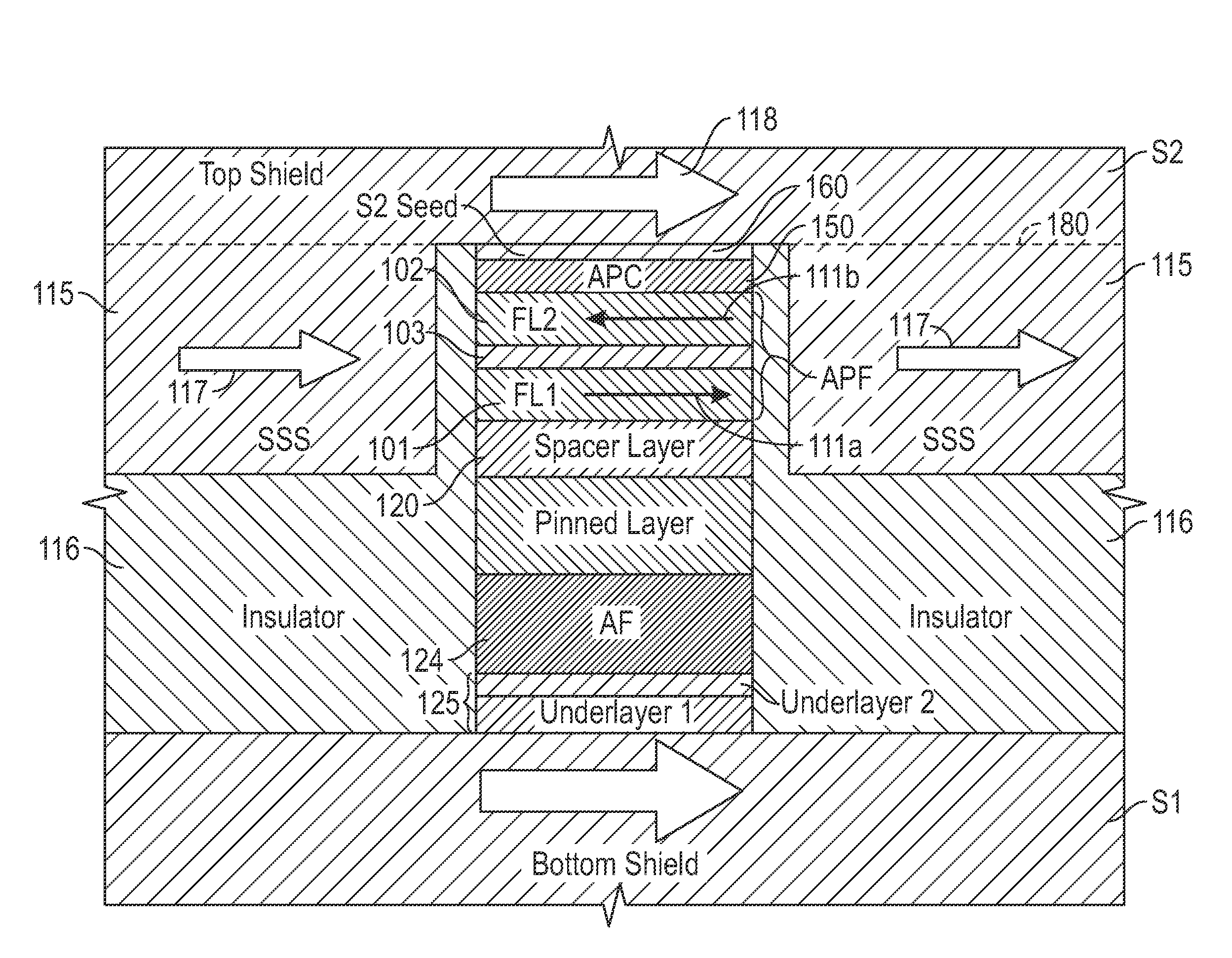
[0034]In embodiments of the invention the FL2 of the APF structure is magnetically coupled antiparallel to the top shield and a top shield seed layer (S2 seed layer) via a nonmagnetic antiparallel coupling (APC) layer. This antiparallel coupling compensates for the opposite coupling to the soft side shields, and therefore improves the magnetic stabilization of FL2. In one embodiment the antiparallel coupling is through an antiferromagnetic-coupling (AFC) layer that provides a dominant antiferromagnetic indirect exchange coupling of FL2 to S2. In another embodiment the antiparallel coupling is by an APC layer that decouples FL2 and S2 and causes the edge-induced magnetostatic coupling between FL2 and the S2 seed layer to dominate. The degree of coupling is controlled by the composition and thickness of the nonmagnetic APC layer between FL2 and the seed layer, and by the thickness of the seed layer. In practice, edge-induced magnetostatic coupling will always be present to some degree...
second embodiment
[0036]FIG. 6 is an enlarged sectional view showing the layers making up the CPP-MR sensor structure according to the invention. The CPP-MR structure is like that of FIG. 4 except that there is no capping layer and there is a nonmagnetic APC layer 155 and ferromagnetic seed layer 165 on FL2 between FL2 and top shield S2. The pinned layer is represented as a simple pinned layer, but alternatively could be an AP-pinned structure like that shown and described in FIG. 4. The APC layer 155 and the S2 seed layer 165 are deposited together with the other layers in the sensor stack as full films so that the coupling properties can be precisely controlled. The APC layer 155 acts as a nonmagnetic spacer layer of sufficient thickness to magnetically decouple FL2 from S2 seed layer 165 and from S2, so that the antiparallel coupling is provided by magnetostatic coupling at the edges of FL2 and seed layer 165, as shown by arrows 170. The APC layer 155 can be formed of any nonmagnetic material, but...
PUM
 Abstract
Description
Claims
Application Information


