Solid-state image sensor and image sensing system

Active Publication Date: 2015-05-14
CANON KK
View PDF5 Cites 8 Cited by
  • Summary
  • Abstract
  • Description
  • Claims
  • Application Information

AI Technical Summary

Benefits of technology

[0008]The present invention provides a technique advantageous in satisfactorily detecting, in a solid-state image sensor capable of detecting light in the first wavelength rang

Problems solved by technology

However, it is difficult to reduce the size and cost.
Furthermore, in the solid-state image sensor described in Japanese Patent Laid-Open No. 2008-005213, since the exposure period (signa

Method used


Image

  • Solid-state image sensor and image sensing system
  • Solid-state image sensor and image sensing system
  • Solid-state image sensor and image sensing system

Examples


Example

First Embodiment

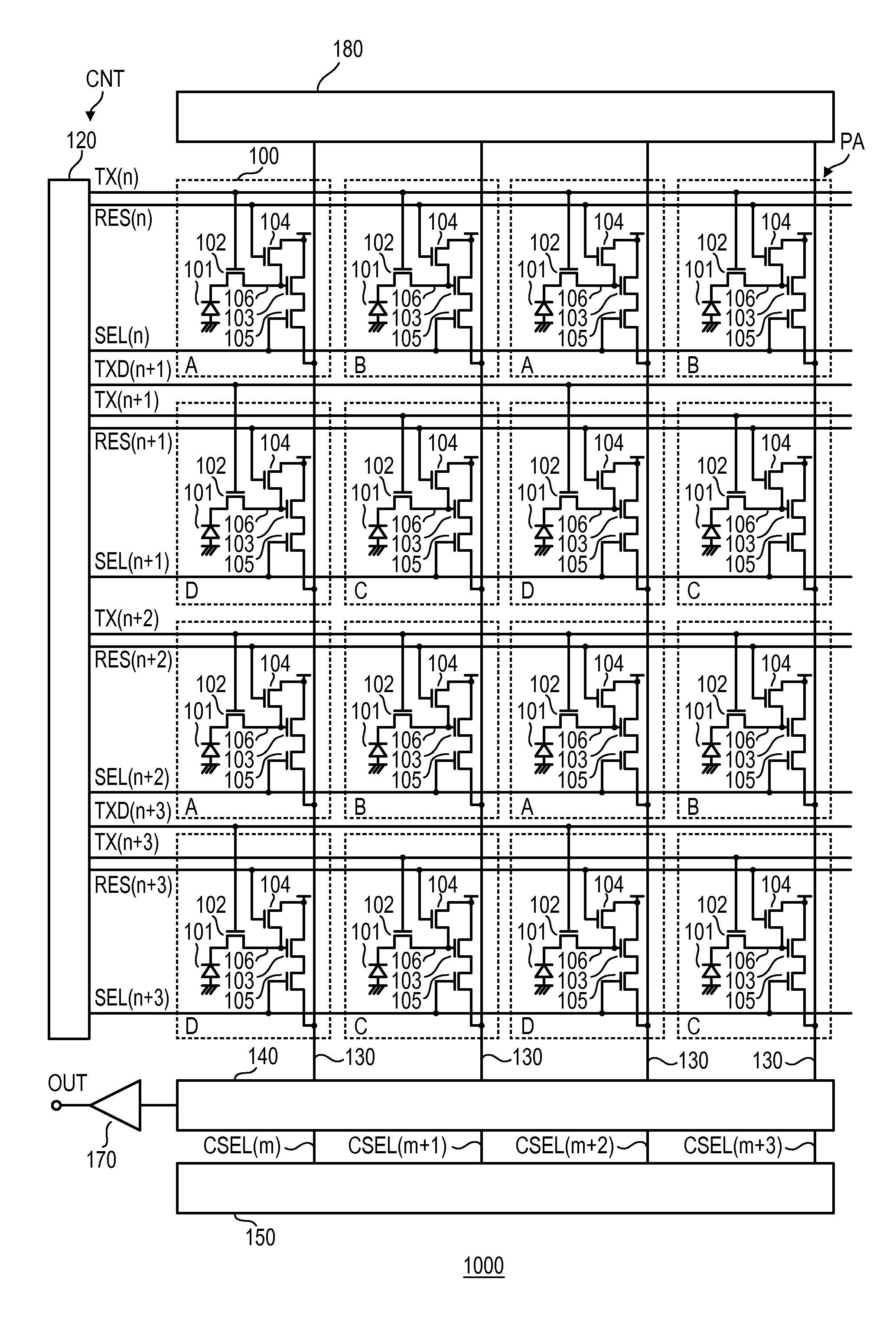
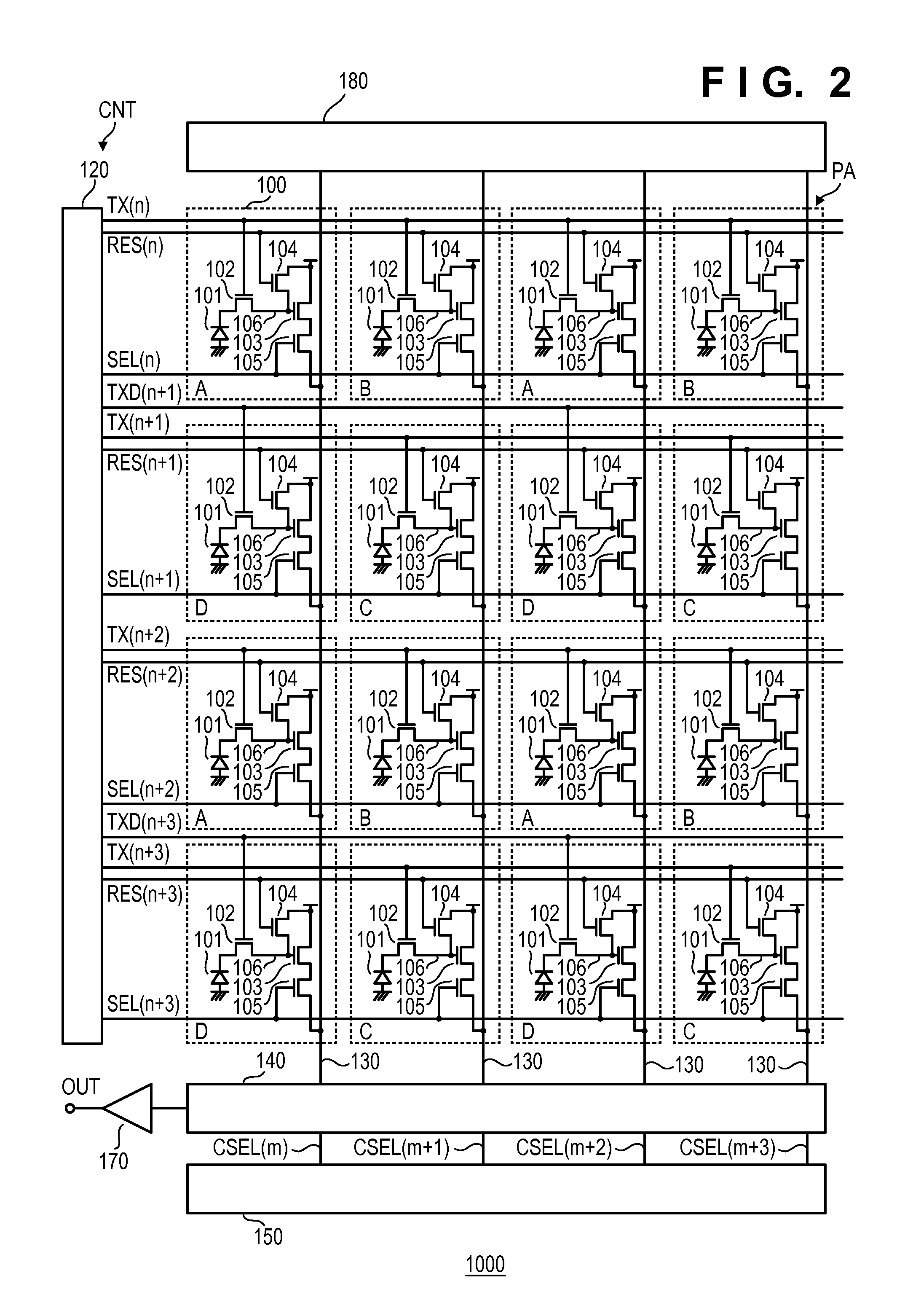
[0022]FIG. 1 shows the arrangement of a pixel array PA of a solid-state image sensor 1000 according to the first embodiment of the present invention. Note that FIG. 1 shows pixels 100 arranged to form a matrix of 4 rows×4 columns for the sake of simplicity. In practice, however, a larger number of pixels 100 are arranged to form a larger number of rows and a larger number of columns. The plurality of pixels 100 of the pixel array PA include A, B, and C pixels as first pixels for detecting light in the first wavelength range, and D pixels as second pixels for detecting light in the second wavelength range including a wavelength range on a longer-wavelength side than the first wavelength range. The A, B, C, and D pixels are respectively indicated by “A”, “B”, “C”, and “D” in FIG. 1 and other drawings. The A, B, and C pixels include color filters which transmit light in different wavelength ranges out of the first wavelength range, respectively. For example, each of the...

Example

Second Embodiment

[0055]A solid-state image sensor 1000 according to the second embodiment of the present invention will be described with reference to FIGS. 5 and 6. Note that details not mentioned in the second embodiment can conform to the first embodiment. In the second embodiment, the solid-state image sensor 1000 outputs an image formed by the signals of first pixels (A, B, and C pixels) (an image frame in the first wavelength range) in a first period P1 (an “image output (A, B, C)” in FIG. 6). The solid-state image sensor 1000 also outputs an image formed by the signals of the first pixels (A, B, and C pixels) and the signals of second pixels (D pixels) (an image frame in the first and the second wavelength ranges) in a second period P2 which is different from the first period P1 (an “image output (A, B, C, D)” in FIG. 6).

[0056]The solid-state image sensor 1000 according to the second embodiment includes transfer control lines TXD(n+1) and TXD(n+3) used for the second pixels (...

Example

Third Embodiment

[0058]A solid-state image sensor 1000 according to the third embodiment of the present invention will be described with reference to FIGS. 7 and 8. Note that details not mentioned in the third embodiment can conform to the first embodiment. The solid-state image sensor 1000 according to the third embodiment includes transfer control lines TXD(n+1) and TXD(n+3) used for second pixels (D pixels) in addition to transfer control lines TX(n), TX(n+1), TX(n+2), and TX(n+3) used for first pixels (A, B, and C pixels). Also, in the solid-state image sensor 1000 according to the third embodiment, each pixel 100 includes a memory portion M. This arrangement makes it possible to read out an image in the first wavelength range and an image in the second wavelength range having different charge accumulation periods in the same frame.

[0059]As illustrated in FIG. 8, in a charge accumulation period in photoelectric converters 101 of the second pixels (D pixels) (indicated as a “charg...


PUM


Abstract

A solid-state image sensor has a plurality of pixels including at least a first pixel configured to detect light in a first wavelength range and a second pixel configured to detect light in a second wavelength range, the second wavelength range including a wavelength range on a longer-wavelength side than the first wavelength range. The sensor includes a control portion configured to supply a control signal to the first and second pixels such that a charge accumulation period of the first pixel is different from a charge accumulation period of the second pixel.

Description

BACKGROUND OF THE INVENTION[0001]1. Field of the Invention[0002]The present invention relates to a solid-state image sensor and an image sensing system.[0003]2. Description of the Related Art[0004]In the observation of a biological body, it is necessary to monitor an image by light in a wavelength range on a short-wavelength side (to be referred to as the first wavelength range hereinafter) and an image by light in a wavelength range on a longer-wavelength side (to be referred to as the second wavelength range) than the first wavelength range at the same time. A method of performing image capturing using an image sensor for the first wavelength range and an image sensor for the second wavelength range, and superimposing the thus obtained images on each other is plausible. However, it is difficult to reduce the size and cost. It is, therefore, necessary to obtain images in two different wavelength ranges using a single image sensor.[0005]Japanese Patent Laid-Open No. 2008-005213 disc...

Claims


Application Information

Patent Timeline
IPC IPC(8): H04N5/372H04N5/378
CPCH04N5/378H04N5/372H04N25/531H04N25/70H04N25/771H04N25/534
Inventor TASHIRO, KAZUAKIOGAWA, KATSUHISA
Owner CANON KK
Why Eureka
Try Eureka