Integrated Circuit Assembly with Faraday Cage

a technology of integrated circuits and faraday cages, which is applied in the direction of electrical equipment, semiconductor devices, semiconductor/solid-state device details, etc., can solve the problems of critical affecting the performance and cost of integrated circuit products, and achieve the effect of reducing the capacitance to ground

Active Publication Date: 2015-05-21
QUALCOMM INC
View PDF3 Cites 58 Cited by
  • Summary
  • Abstract
  • Description
  • Claims
  • Application Information

AI Technical Summary

Benefits of technology

[0011]In some embodiments, the electrically conductive ring is above the region of the semiconductor layer in which the active device is formed. In other embodiments, the electrically conductive ring is below this region of the semiconductor layer. In some embodiments, one or more additional electrically conductive rings are formed above or below this region. Each electrically conductive ring may have an opening through which an electrically conductive connection line may electrically connect the active device wit

Problems solved by technology

The nature of this metal interconnect critically affects t

Method used


Image

  • Integrated Circuit Assembly with Faraday Cage
  • Integrated Circuit Assembly with Faraday Cage
  • Integrated Circuit Assembly with Faraday Cage

Examples


Embodiment Construction

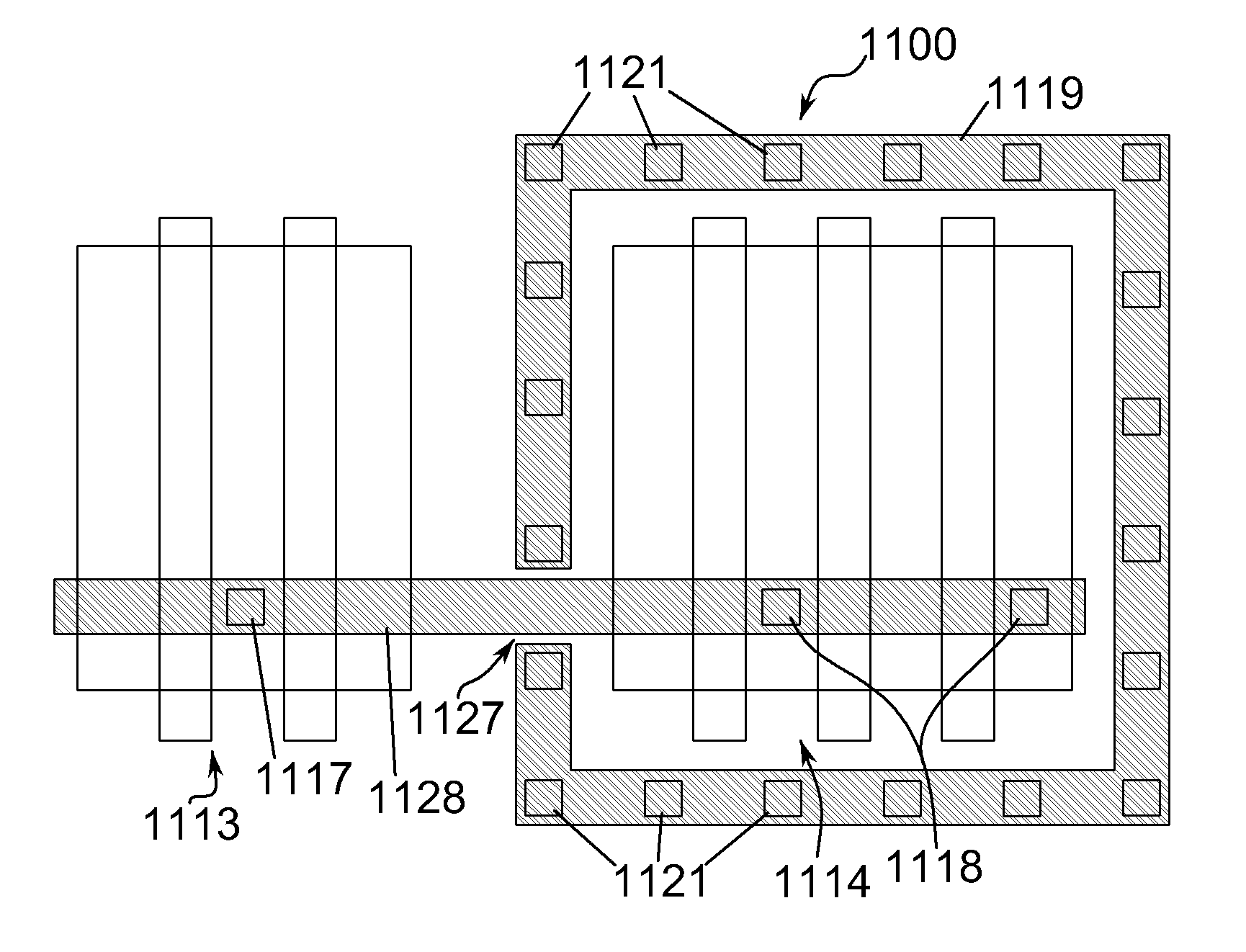
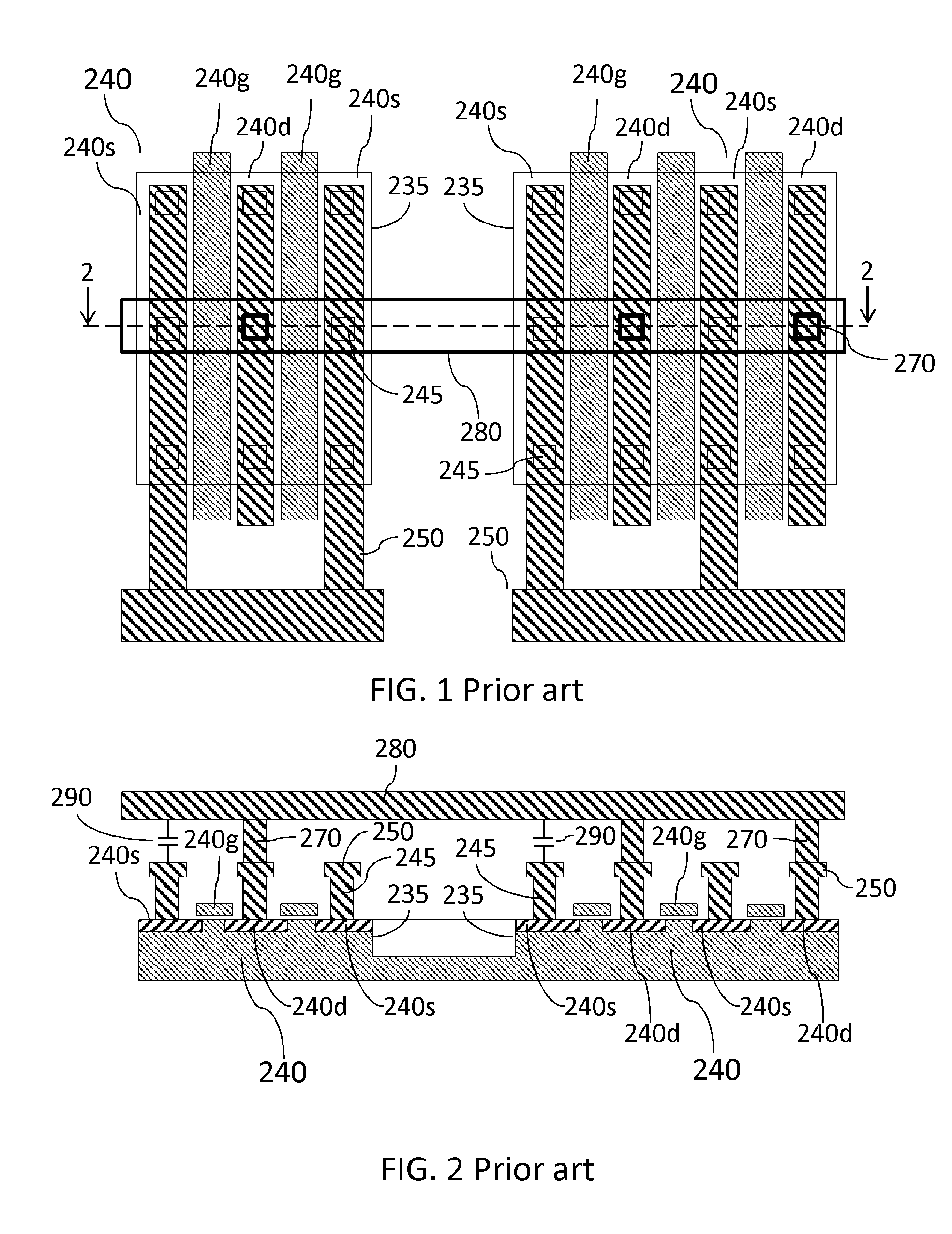
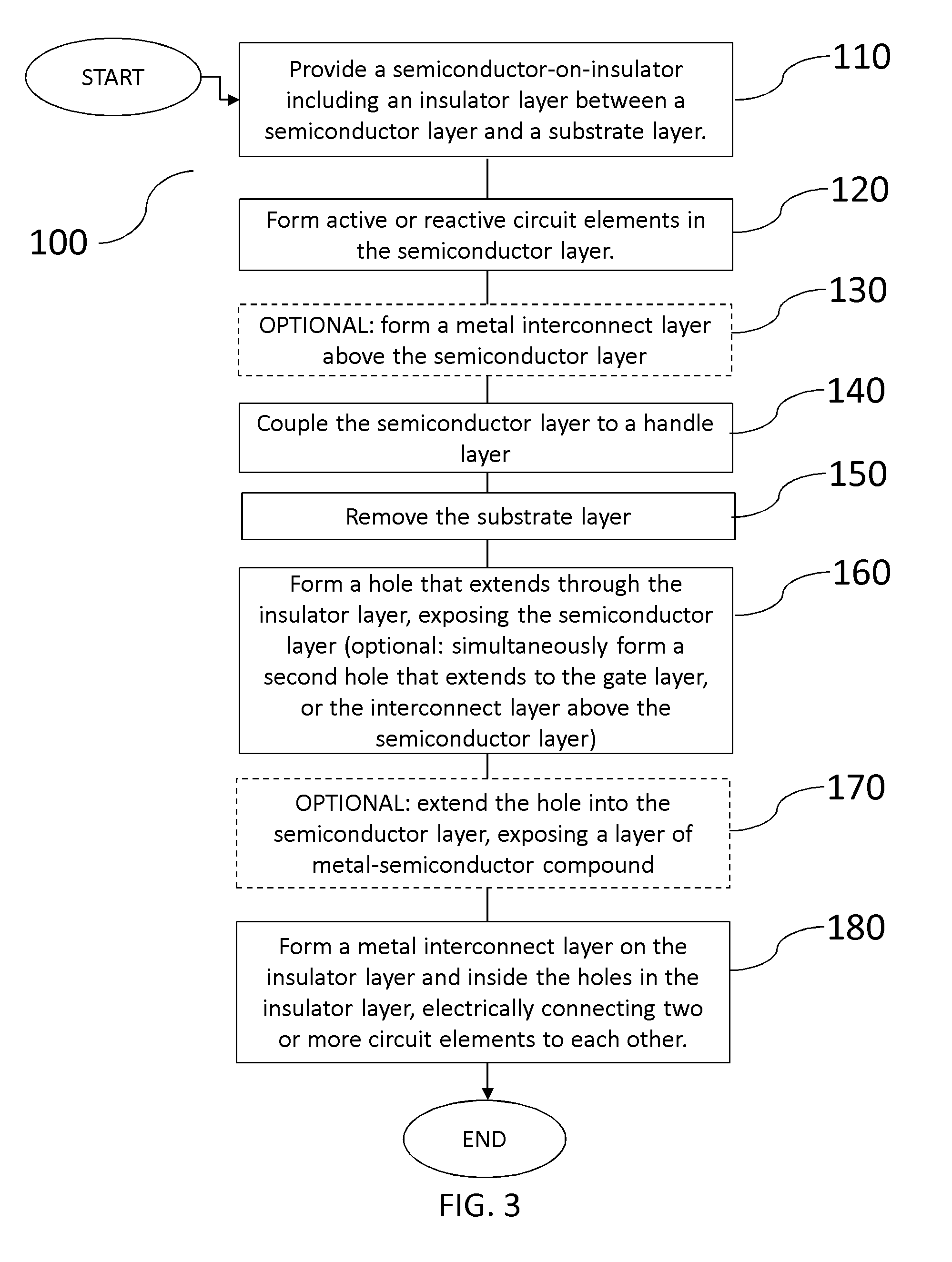
[0026]High-speed, high performance integrated circuits are often fabricated using silicon-on-insulator (SOI) technologies. SOI technologies also lend themselves to layer-transfer techniques, where the active layer of the SOI is transferred, using bonding and etch-back methods, to a different substrate. This method may have advantages of lower capacitance and higher speed, easier thermal management, and easier access to the body regions of SOI transistors. An example of such a process is described in U.S. Pat. No. 8,357,935 entitled, “Silicon-on-insulator with back side connection”, owned by the assignee of the present application and filed on Apr. 28, 2012, which is incorporated herein by reference in its entirety. Layer transfer techniques may also be used to form circuits on fully insulating or transparent substrates, which may be advantageous in opto-electronic applications, for example.

[0027]Transferring the active layer of an integrated circuit also can expose the surface of th...


PUM


Abstract

An integrated circuit assembly is formed with an insulating layer, a semiconductor layer, an active device, first, second, and third electrically conductive interconnect layers, and a plurality of electrically conductive vias. The insulating layer has a first surface and a second surface. The second surface is below the first surface. A substrate layer has been removed from the second surface. The semiconductor layer has a first surface and a second surface. The first surface of the semiconductor layer contacts the first surface of the insulating layer. The active device is formed in a region of the semiconductor layer. The first electrically conductive interconnect layer forms an electrically conductive ring. The second electrically conductive interconnect layer forms a first electrically conductive plate above the electrically conductive ring and the region of the semiconductor layer. The third electrically conductive interconnect layer forms a second electrically conductive plate below the electrically conductive ring and the region of the semiconductor layer. The plurality of electrically conductive vias electrically couple the electrically conductive ring to the first electrically conductive plate and to the second electrically conductive plate. The electrically conductive ring, the first electrically conductive plate, the second electrically conductive plate, and the plurality of electrically conductive vias form a Faraday cage around the active device.

Description

CROSS-REFERENCE TO RELATED APPLICATIONS[0001]This application is a continuation-in-part of U.S. application Ser. No. 14 / 272,261, filed May 7, 2014, which is a continuation of U.S. patent application Ser. No. 13 / 851,926, now U.S. Pat. No. 8,748,245, filed Mar. 27, 2013, all of which are hereby incorporated by reference herein in their entirety for all purposes. This application also relates to the disclosure in U.S. application Ser. No. 14 / 451,342, filed Aug. 4, 2014, which is hereby incorporated by reference herein in its entirety for all purposes.BACKGROUND OF THE INVENTION[0002]In an integrated circuit, metal lines typically connect individual circuit elements together. The nature of this metal interconnect critically affects the performance and cost of the integrated circuit product. For example, most integrated circuit processes offer multiple levels of metal interconnect, in order to allow the maximum flexibility in circuit layout. This layout flexibility allows a designer to m...

Claims


Application Information

Patent Timeline
IPC IPC(8): H01L21/768H01L23/60H01L23/48
CPCH01L21/76895H01L23/60H01L23/481H01L21/84H01L27/1203H01L2924/0002H01L23/5225H01L21/76898H01L2924/00H01L21/76251H01L23/5226H01L23/528H01L23/552
Inventor STUBER, MICHAEL A.
Owner QUALCOMM INC
Why Eureka
Try Eureka