Display device and method of manufacturing display device

Active Publication Date: 2015-06-04
JOLED INC
View PDF4 Cites 3 Cited by
  • Summary
  • Abstract
  • Description
  • Claims
  • Application Information

AI Technical Summary

Benefits of technology

The present invention provides a display device and a method to make it that can fix short circuiting without making the wiring more resistant.

Problems solved by technology

As such, when a conductive foreign object or a pinhole is formed between the wires having different potentials in the manufacturing process, an interwire short circuit may occur which could hinder panel driving and cause deterioration of panel yield.

Method used


Image

  • Display device and method of manufacturing display device
  • Display device and method of manufacturing display device
  • Display device and method of manufacturing display device

Examples


embodiment 1

[0037]Hereinafter, a display device according to Embodiment 1 is described using FIG. 6 to FIG. 8.

[0038][1-1. Structure of Display Device]

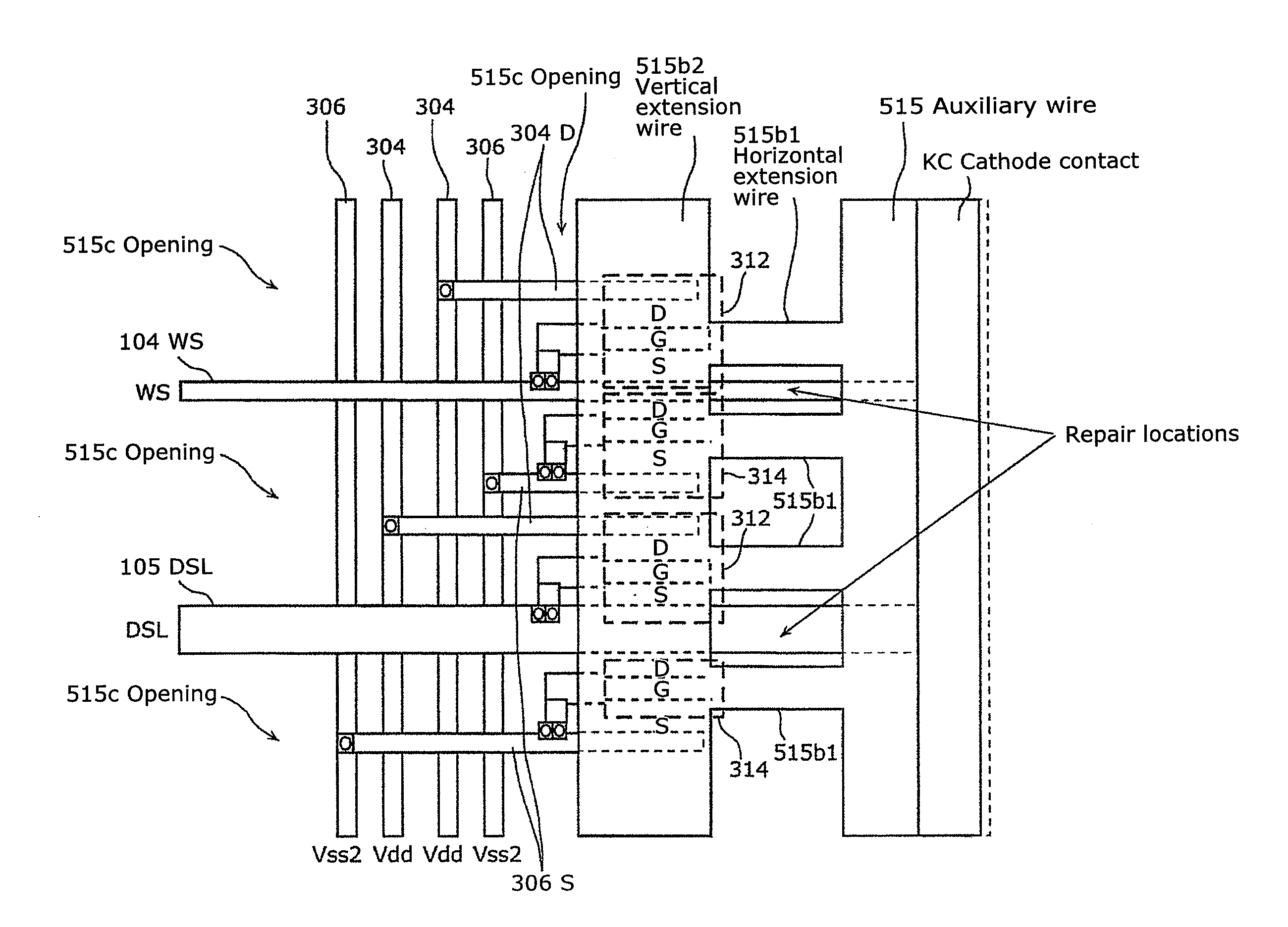
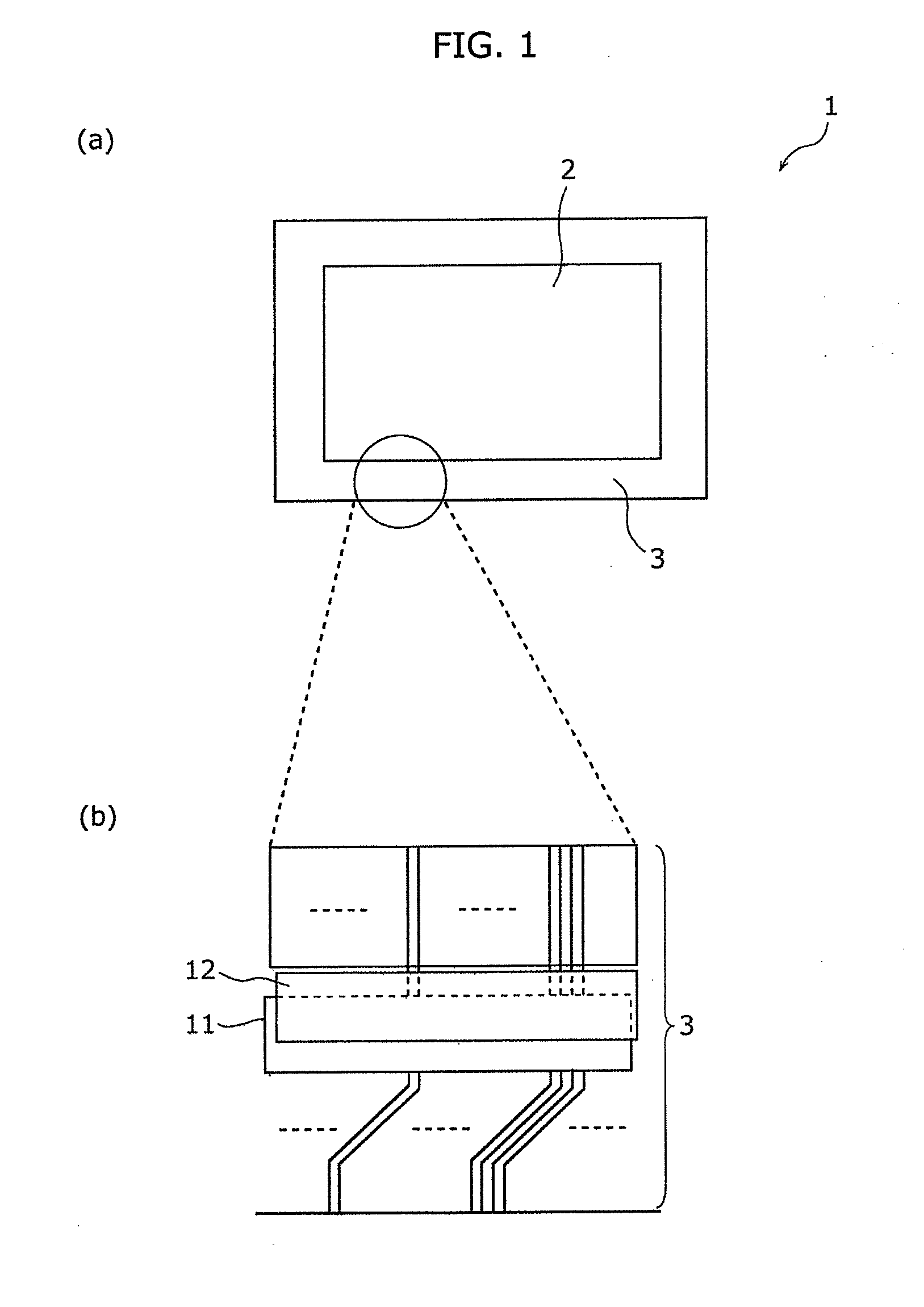
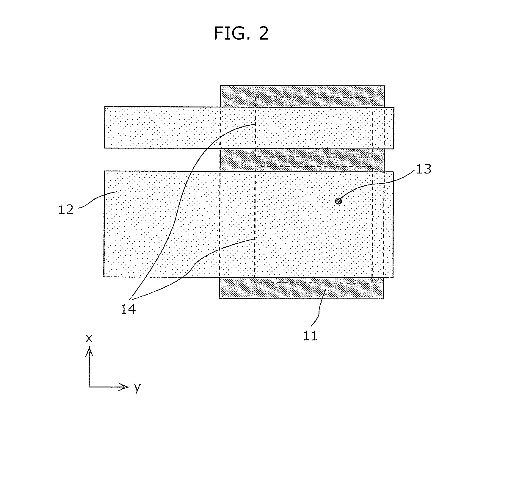
[0039]FIG. 6 is top view of a panel periphery of the display device 1 according to this embodiment; (b) illustrates a portion at which wide wires three-dimensionally cross each other, and (a) is an enlarged view of a portion of (b). FIG. 7 is a top view of a panel periphery of a display device according to the present embodiment.

[0040]As in the display device 1 illustrated in (a) in FIG. 1, the display device 1 according to the present embodiment includes the display area 2 and the panel periphery 3. Pixels each including, for example, a display element such as an organic EL element and a pixel circuit such as a drive transistor are arranged in a matrix in the display area 2. Furthermore, as in the display device illustrated in (b) in FIG. 1, the lower wiring layer 11 and the upper wiring layer 12 are arranged in the panel periphery 3. For example...

embodiment 2

[0080]Next, Embodiment 2 is described below. A display device according to this embodiment is different from the display device according to Embodiment 1 in terms of the structure of the first electrode and the second electrode. Hereinafter, Embodiment 2 is described using FIG. 9.

[0081][2-1. Structure of Display Device]

[0082]FIG. 9 is a top view of a panel periphery of the display device according to the present embodiment.

[0083]As illustrated in FIG. 9, a first power supply line 211 which is the first electrode according to this embodiment includes first partial electrode portions 211a, first cuttable portions 211b, first openings 211c, and first connecting electrode portions 211d. Furthermore, a second power supply line 211 which is the second electrode according to this embodiment includes second partial electrode portion 212a, second cuttable portions 212b, second openings 212c, and second connecting electrode portions 212d. The first connecting electrode portions 211d and the s...


PUM


Abstract

A display device includes a lower wiring layer, an interlayer insulating layer, and an upper wiring layer. The lower wiring layer includes first partial electrode portions, first cuttable portions, and first openings; the upper wiring layer includes second partial electrode portions, second cuttable portions, and second openings. The first partial electrode portions and the second partial electrode portions are disposed in overlapping positions in the stacking direction; all the first cuttable portions and the second openings are disposed in overlapping positions in the stacking direction; all the second cuttable portions and the first openings are disposed in overlapping positions in the stacking direction.

Description

TECHNICAL FIELD[0001]The present disclosure relates to display devices and methods of manufacturing a display device.BACKGROUND ART[0002]In general, display devices have a structure in which wires having different potentials are stacked in a panel periphery in which electronic elements such as thin-film transistors are arranged. For example, a display device has a structure in which a first power supply line for supplying power supply voltage to a thin-film transistor and a second power supply line for supplying, to an organic EL element, a voltage different from the voltage supplied by the first power supply line are stacked via an insulating film. As such, when a conductive foreign object or a pinhole is formed between the wires having different potentials in the manufacturing process, an interwire short circuit may occur which could hinder panel driving and cause deterioration of panel yield.[0003]In order to avoid such a problem, a wiring layout that allows an interwire short ci...

Claims


Application Information

Patent Timeline
IPC IPC(8): H01L27/12H01L51/56H01L51/00H01L27/32
CPCH01L27/124H01L27/3248H01L51/0031H01L51/56H01L51/0021H01L27/3276G02F1/136259G02F1/136263H10K71/60H10K71/621H10K71/70H10K59/131H10K71/861H10K59/123H10K71/00
Inventor MATSUI, MASAFUMIEBISUNO, KOUHEI
Owner JOLED INC
Why Eureka
Try Eureka