Imaging device

a technology of imaging device and lens, which is applied in the direction of instruments, focusing aids, lenses, etc., can solve the problems of increasing manufacturing cost and increasing manufacturing cost, and achieve the effect of dramatically increasing the number of taken images at different focal distances that are simultaneously obtainabl

Active Publication Date: 2015-06-04
FUJIFILM CORP
View PDF7 Cites 38 Cited by
  • Summary
  • Abstract
  • Description
  • Claims
  • Application Information

AI Technical Summary

Benefits of technology

[0009]The present invention was made in view of these circumstances, and has an object of providing an imaging device capable of dramatically increasing the number of taken images at different focal distances that are simultaneously obtainable, without increasing difficulty in manufacture, the imaging device that can be manufactured at low cost.
[0011]According to the one aspect of the present invention, by combining the multifocal main lens and the multifocal microlens array, the number of taken images at different focal distances that are simultaneously obtainable can be dramatically increased. Also, for the plurality of images at different focal distances, the number of (types of) focal distances of the multifocal main lens and the number of (types of) focal distances of the multifocal microlens array can be decreased. With this, an increase in manufacturing cost of the multifocal main lens and the multifocal main lens array can be prevented.
[0013]In the imaging device according to still another aspect of the present invention, when the number of focal points of the multifocal main lens is taken as m and the number of focal points of the multifocal microlens array is taken as n, the image obtaining device obtains m×n images at different focal distances. With this, compared with the number of focal points, m, of the multifocal main lens and the number of focal points, n, of the multifocal microlens array, the number of taken images (m×n) at different focal distances that are simultaneously obtainable can be dramatically increased.
[0021]According to the present invention, the multifocal main lens and the multifocal microlens array are combined, and a plurality of images for each focal distance obtained by combining the multifocal main lens and a plurality of microlens groups at different focal distances are each obtained. Therefore, the number of taken images at different focal distances that are simultaneously obtainable can be dramatically increased.

Problems solved by technology

However, if the number of types of lens sets is increased, difficulty in manufacturing the microlens array is increased, thereby causing an increase in manufacturing cost.
However, if the number of focal points of the main lens is increased, difficulty in manufacturing the main lens is increased, thereby causing an increase in manufacturing cost.

Method used


Image

  • Imaging device
  • Imaging device
  • Imaging device

Examples


first embodiment

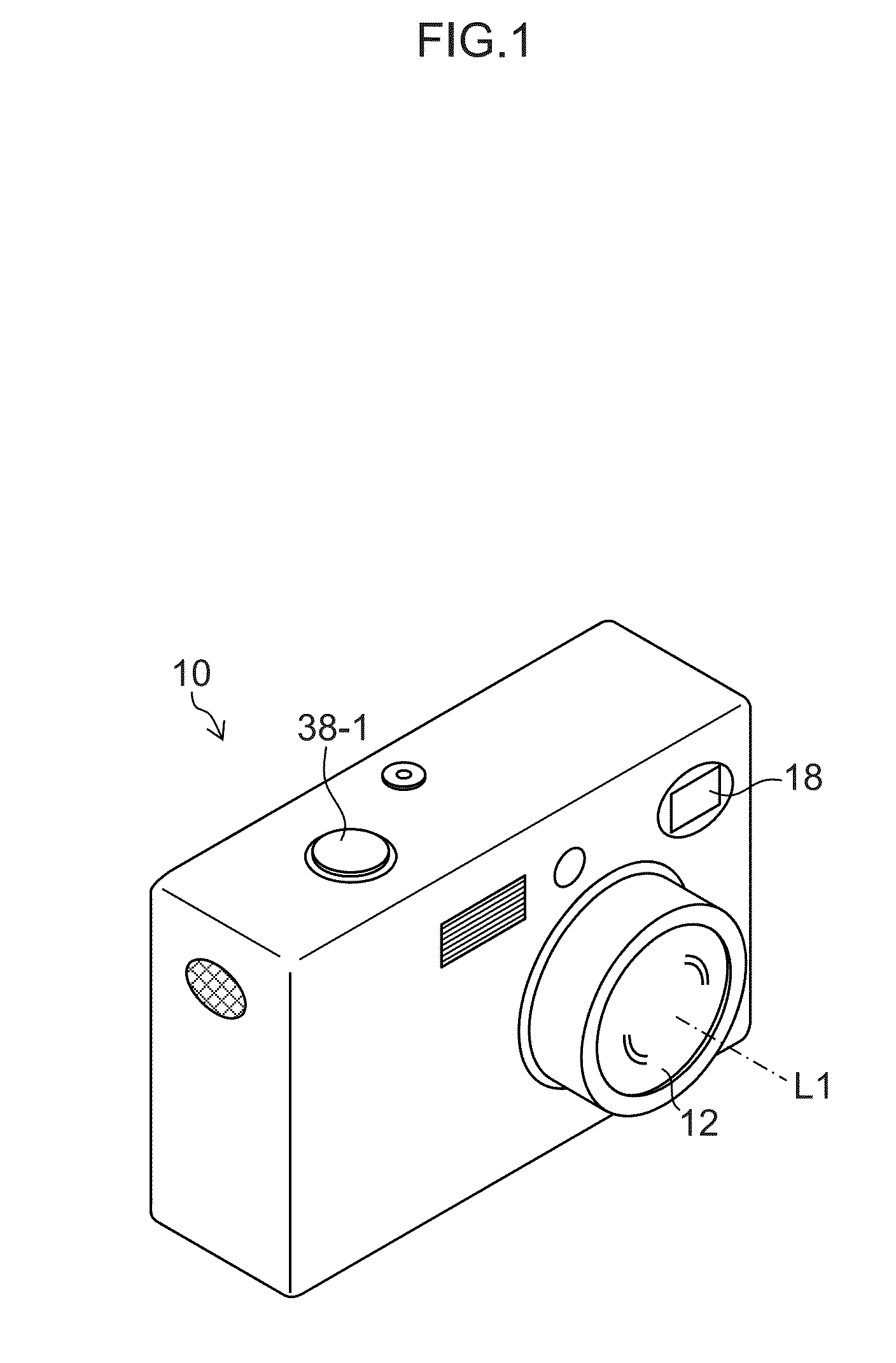
[0050]FIG. 1 is an external perspective view of an imaging device 10 (imaging device) according to the present invention. As depicted in FIG. 1, a taking lens (multifocal main lens) 12, a stroboscope 18, and others are arranged on a front surface of the imaging device 10, and a shutter button 38-1 is provided on an upper surface thereof. L1 denotes an optical axis of the multifocal main lens 12.

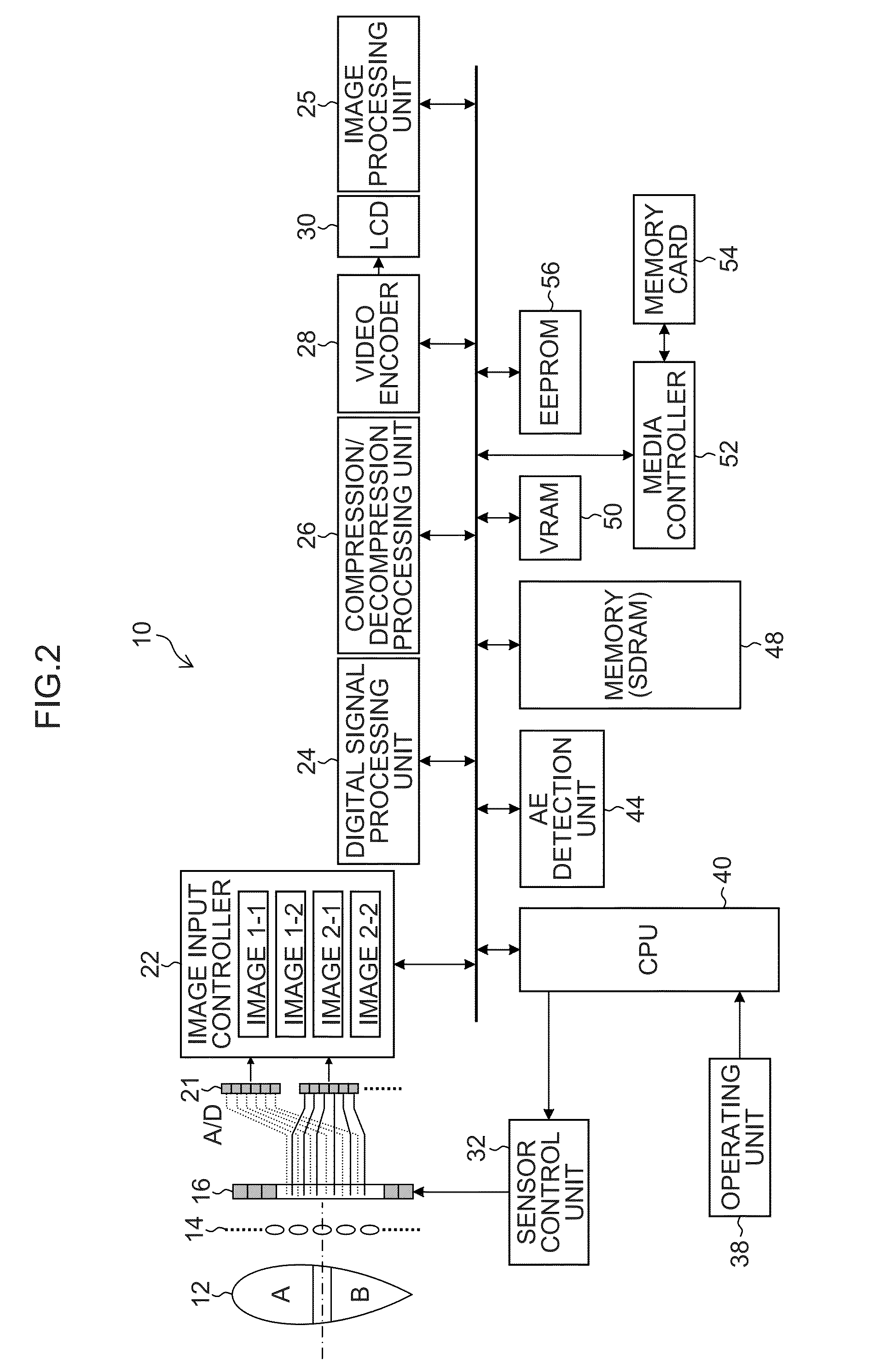
[0051]FIG. 2 is a block diagram depicting an embodiment of an inner structure of the imaging device 10.

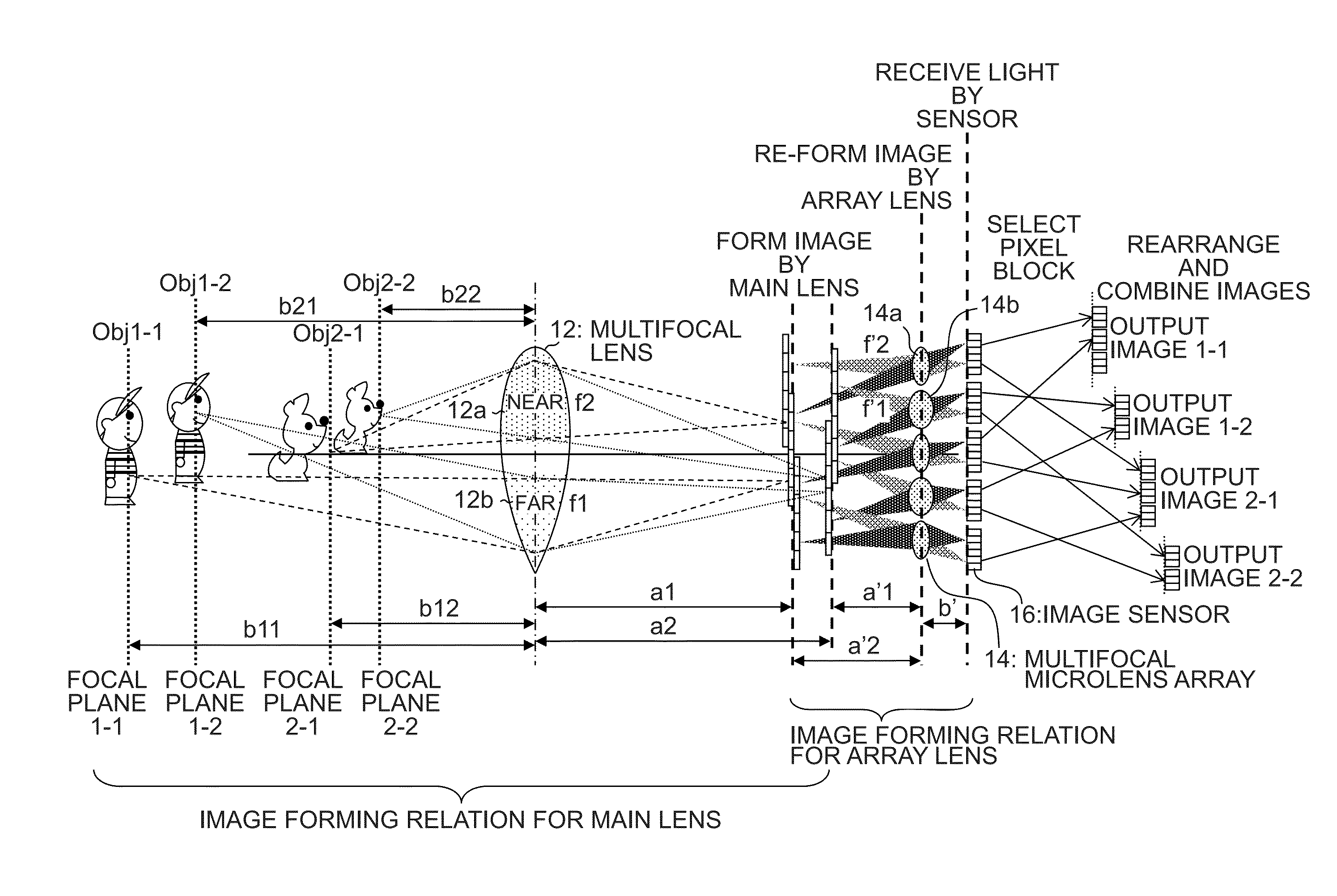
[0052]This imaging device 10 records a taken image in a memory card 54, and has an imaging optical system for a so-called plenoptic camera, with a multifocal microlens array 14 provided between the multifocal main lens 12 and a CMOS-type image pickup element (image sensor) 16. The operation of the device as a whole is controlled in a centralized manner by a central processing unit (CPU) 40.

[0053]The imaging device 10 is provided with an operating unit 38 including the shutter button 38-1, a ...

second embodiment

[0098][Second Embodiment of Multifocal Microlens Array]

[0099]FIG. 8 is a diagram depicting a second embodiment of the multifocal microlens array.

[0100]A multifocal microlens array 114 has two microlens groups 114a and 114b with different focal lengths, and each lens is formed so as to have a one-to-one correspondence with each light-receiving cell 16a of the image sensor 16.

[0101]Since each lens of the multifocal microlens array 114 has a one-to-one correspondence with each light-receiving cell 16a of the image sensor 16, a microprism array 110 is provided as a control device for restricting the direction of light beams incident to each light-receiving cell 16a.

[0102]That is, the microprism array 110 is provided on a front surface (a multifocal main lens 12 side) of the multifocal microlens array 114. The microprism array 110 has two types of prism groups 110a and 110b which refract incident light beams in different refracting directions. With this microprism array 110, the positio...

third embodiment

[0113][Third Embodiment of Multifocal Microlens Array]

[0114]FIG. 11 is a side view depicting a third embodiment of the multifocal microlens array. A multifocal microlens array 214 depicted in FIG. 11 has two microlens groups, that is, a microlens group 214a and a microlens group 214b with different lens positions (heights) in an optical axis direction. With this, the microlens group 214a and the microlens group 214b have different focal distances.

[0115][Number of Lenses of Microlens Group of Multifocal Microlens Array]

[0116]FIG. 12 is a graphical overview of an embodiment of weighting the number of lenses of two microlens groups with different focal lengths of the multifocal microlens array.

[0117]A multifocal microlens array 314 depicted in FIG. 12 has a microlens group 314a and a microlens group 314b with different focal lengths. The microlens group 314a and the microlens group 314b each have a different number of lenses. For one lens of the microlens group 314b, eight surrounding ...


PUM


Abstract

An imaging device includes a multifocal main lens having different focal distances for a plurality of regions, an image sensor having a plurality of pixels configured of two-dimensionally arranged photoelectric converting elements, a multifocal lens array having a plurality of microlens groups at different focal distances disposed on an incident plane side of the image sensor, and an image obtaining device which obtains from the image sensor, a plurality of images for each of the focal distances obtained by combining the multifocal main lens and the plurality of microlens groups at different focal distances.

Description

CROSS-REFERENCE TO RELATED APPLICATIONS[0001]This application is a Continuation of PCT International Application No. PCT / JP2013 / 070725 filed on Jul. 31, 2013, which claims priority under 35 U.S.C§119(a) to Japanese Patent Application No. 2012-174288 filed on Aug. 6, 2012. Each of the above application(s) is hereby expressly incorporated by reference, in its entirety, into the present application.BACKGROUND OF THE INVENTION[0002]1. Field of the Invention[0003]The present invention relates to imaging devices and, in particular, relates to an imaging device capable of simultaneously obtaining a plurality of images with different focal subject distances.[0004]2. Description of the Related Art[0005]Conventionally, as a microlens array configuring a plenoptic camera, an image input device has been suggested, in which a microlens array configured of a plurality of lens sets at different focal distances is provided on a front surface side of an image pickup element and images are re-formed ...

Claims


Application Information

Patent Timeline
Patent Type & Authority Applications(United States)
IPC IPC(8): H04N13/02H04N13/232
CPCH04N13/0228G02B3/0006G02B3/10H04N13/0282G02B3/0043G02B3/14G02B5/06G02B7/343G02B7/38G02B27/0075G03B13/36H01L27/14627H04N13/232H01L27/14623H04N23/957H04N13/229H04N13/282
Inventor ONO, SHUJI
Owner FUJIFILM CORP
Why Eureka
Try Eureka