Use of Shear to Incorporate Tilt into the Microstructure of Reversible Gecko-Inspired Adhesives
a technology of reversible gecko and microstructure, applied in the direction of film/foil adhesives, mechanical equipment, transportation and packaging, etc., can solve the problems of not showing anisotropic adhesion or relying on multi-step, expensive fabrication schemes, and not being easily scalable for hierarchical structures
- Summary
- Abstract
- Description
- Claims
- Application Information
AI Technical Summary
Benefits of technology
Problems solved by technology
Method used
Image
Examples
example 1
[0038]Fabrication of Patterned Silicon Mold
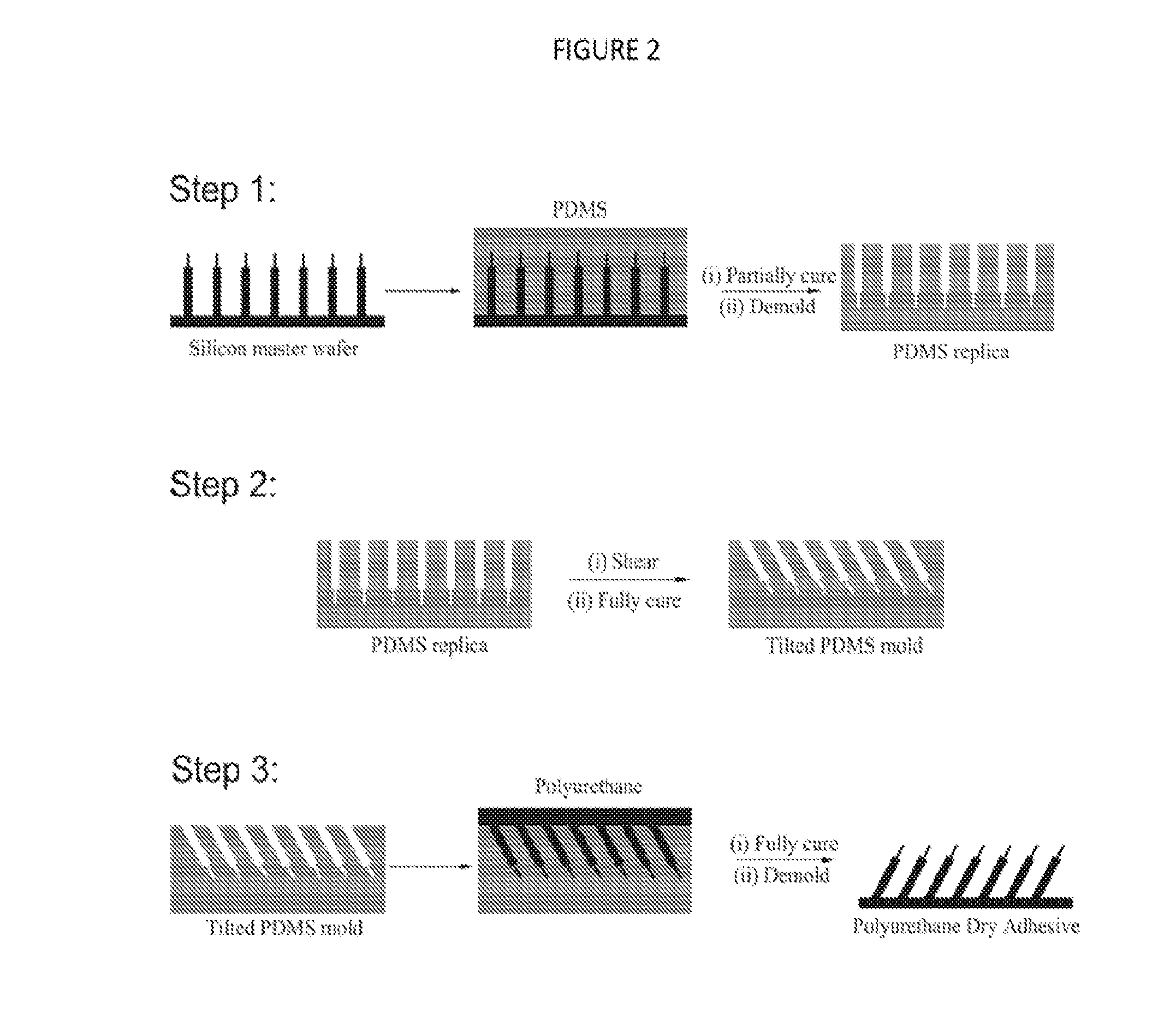
[0039]Silicon master wafers were fabricated using standard microfabrication techniques. Briefly, four-inch silicon wafers (Test grade, University Wafers) were cleaned in an oxygen plasma, after which a 600 nm oxide layer was grown using plasma-enhanced chemical vapor deposition. Next, positive photoresist was spun onto the wafers (Shipley 1813), patterned with rectangular structures mimicking the gecko spatulae, and developed. The oxide layer was then opened by reactive ion etching with CF4. The patterned oxide layer formed the bottom of the two-layer etch mask. The remaining photoresist was stripped off, and a new layer of Shipley 1818 was spun onto the wafers. This new layer was patterned with cylindrical structures mimicking the gecko setae and developed. The photoresist layer formed the top of the two-layer etch mask. Once the two-layer etch mask was in place, the hierarchical structure itself was formed using deep reactive ion etching....
example 2
[0060]In an alternative embodiment, the polyurethane-based gecko-inspired structures consist of 2 levels of hierarchy (see FIG. 11A); a triangular prism pillar (approximately 30 μm×25 μm×25 μm, and 80 μm high) terminated by a rectangular pad-like structure (approximately 20 μm×20 μm×7 μm), arranged in a rectangular lattice (approximately 30 μm center-to-center in the tilt (x-axis) direction, and 37 μm center-to-center along the in-plane or y-axis axis).
[0061]Fabrication of Patterned Silicon Mold
[0062]Silicon master wafers were fabricated using standard microfabrication techniques. Briefly, 4 inch silicon wafers (test grade, University Wafers) were cleaned in an oxygen plasma, after which a 600 nm oxide layer was grown using plasma-enhanced chemical vapor deposition. Next, positive photoresist was spun onto the wafers (Shipley 1813), patterned with rectangular structures mimicking the gecko spatulae, and developed. The oxide layer was then opened by reactive ion etching with CF4. The...
PUM
| Property | Measurement | Unit |
|---|---|---|
| Thickness | aaaaa | aaaaa |
| Thickness | aaaaa | aaaaa |
| Diameter | aaaaa | aaaaa |
Abstract
Description
Claims
Application Information


