Liquid crystal display device

Active Publication Date: 2015-06-11
JAPAN DISPLAY INC
View PDF2 Cites 9 Cited by
  • Summary
  • Abstract
  • Description
  • Claims
  • Application Information

AI Technical Summary

Benefits of technology

[0028]According to the present invention, a liquid crystal display device using a high-definition screen to thereby reduce the area of each pixel and also using an organic passivation film in a TFT substrate is provided, which can stably form an alignment film in a through-hole, even if a through-

Problems solved by technology

Thus the material of the alignment film becomes difficult to flow into the through-hole.
Consequently, a display defect, such as a luminance unevenness, occurs.
Consequently, it is difficult to form a height difference among the surrounding portions of the throu

Method used


Image

  • Liquid crystal display device
  • Liquid crystal display device
  • Liquid crystal display device

Examples


Example

First Embodiment

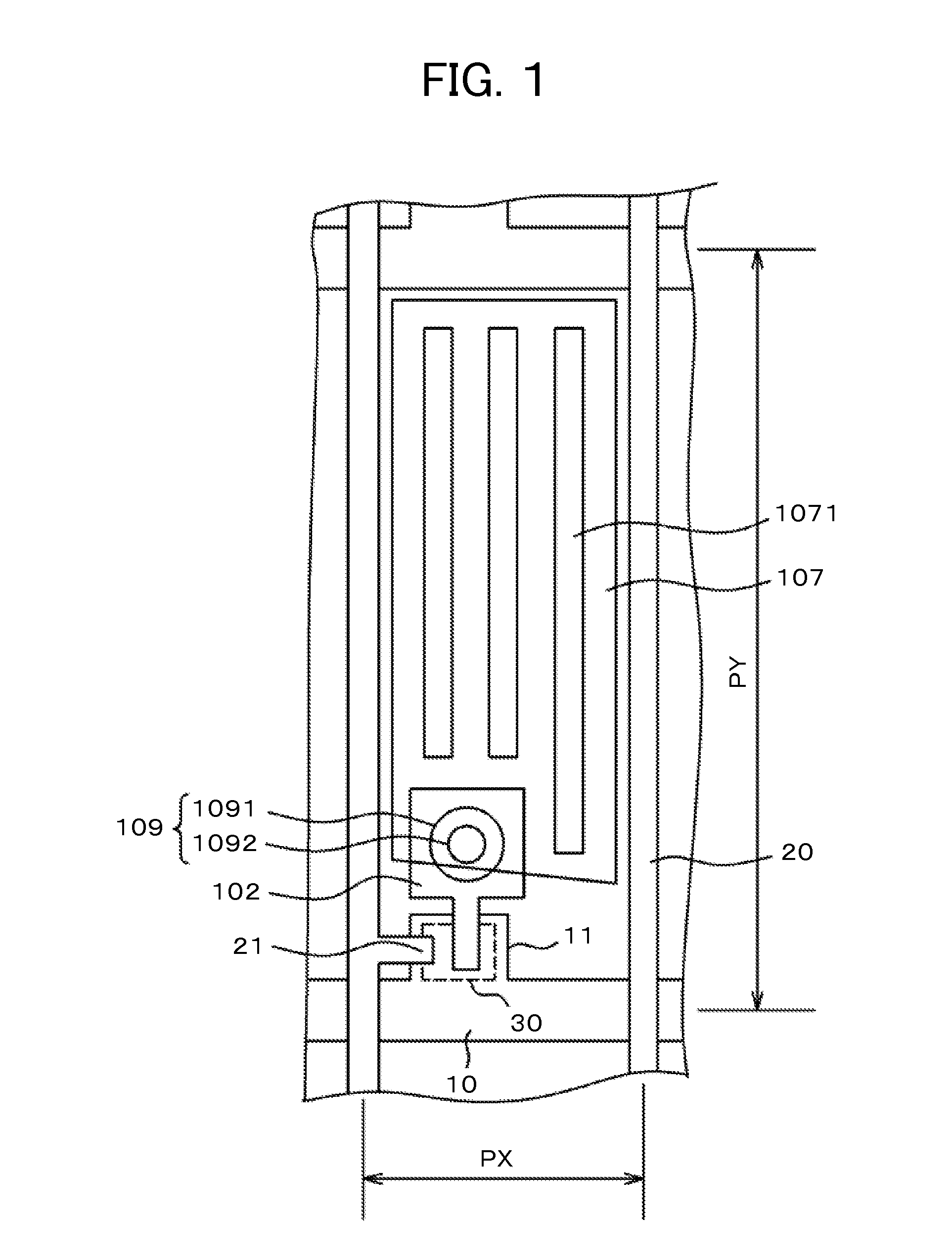
[0047]FIG. 1 is a plan view of a pixel in a TFT substrate of a liquid crystal display device to which the present invention is applied. FIG. 1 illustrates an example of an IPS liquid crystal display device. In FIG. 1, scanning lines 10 extend in a lateral direction and are arranged in a longitudinal direction at a predetermined pitch PY. Video signal lines 20 extend in the longitudinal direction and are arranged in the lateral direction at a predetermined pitch PX. Each region surrounded by the scanning line 10 and the video signal line 20 is a pixel.

[0048]In FIG. 1, a gate electrode 11 branches from the scanning line 10. A semiconductor layer 30 is formed on the gate electrode 11. On the other hand, a source electrode 102 is formed on the semiconductor layer 30. The source electrode 102 extends in the direction of a pixel electrode 107 and increases in width at part thereof overlapping with a pixel electrode 106 and under a through-hole 109. The source electrode 10...

Example

Second Embodiment

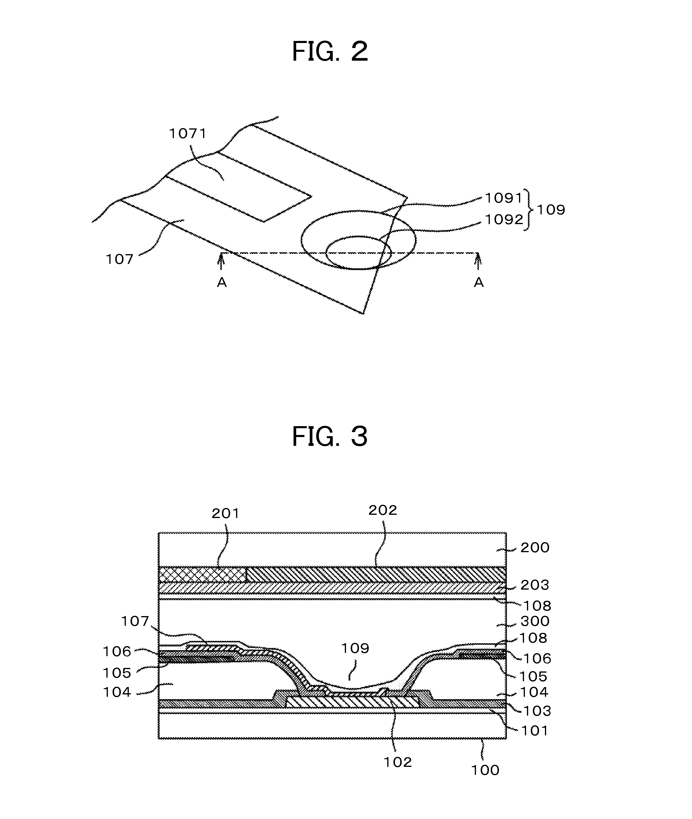
[0060]FIG. 6 is a perspective view illustrating a relationship between a pixel electrode 107 and a through-hole 109 according to a second embodiment of the present invention. In FIG. 6, a slit 1071 formed in a pixel electrode 10 extends in a through-hole 109. In the slit 1071, a surface thereof is formed of SiN configuring an interlayer insulating film 106, instead of ITO. Thus, an alignment film material 108 of a liquid form can flow into the through-hole 109, starting from a boundary portion of a step-like part of the ITO film. Further, because the surface is formed of the SiN film in the slit 1071, the alignment film material 108 is easier to wet and spread in this case than a case of using the ITO film. Thus, also from this aspect, the alignment film material 108 is easier to flow into the through-hole 109.

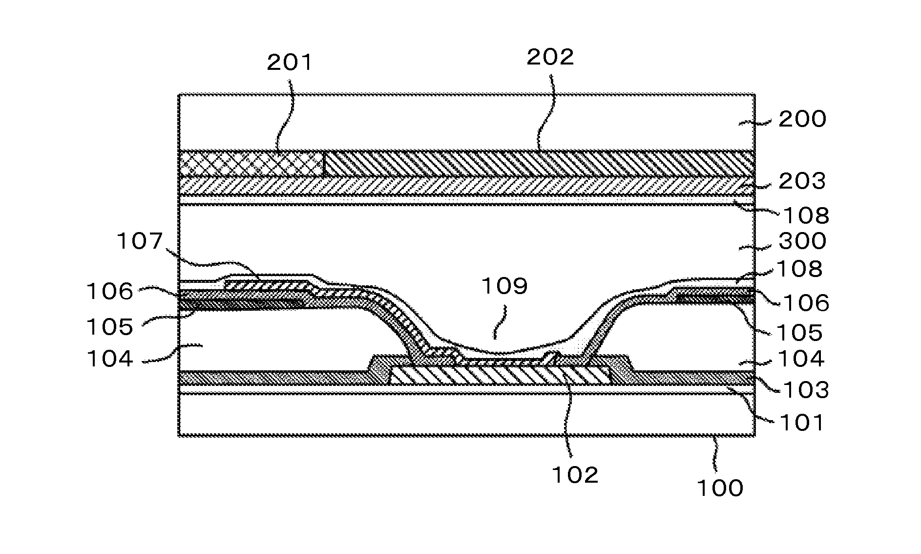
[0061]FIG. 7 is a cross-sectional view of a liquid crystal display device, which corresponds to a cross-section taken on line E-E shown in FIG. 6. FIG. 7 is s...

Example

Third Embodiment

[0066]A third embodiment is an IPS liquid crystal display device configured so that a pixel electrode 107 formed in a planar and solid manner is arranged on a lower side, and that a common electrode 105 having a slit 1051 is provided on an upper side via an interlayer insulating film 106, contrary to the first embodiment.

[0067]FIG. 10 is a perspective view illustrating a relationship between a common electrode 105 and a through-hole 109 according to the third embodiment. In FIG. 10, the common electrode 105 having the slit 1051 does not cover the entire inner wall of the through-hole 109. In an outside of the common electrode 105, the common electrode 105 does not cover the inner wall and the periphery of the top face of the through-hole 109.

[0068]FIG. 11 is a cross-sectional view of the liquid crystal display device, which corresponds to the cross-section taken on line G-G shown in FIG. 10. The common electrode 105 is formed on a left-side periphery and a left-side ...


PUM


Abstract

To prevent a phenomenon that an alignment film material is difficult to flow into the through-hole where a diameter of a through-hole for connecting between a pixel electrode and a source electrode is reduced.
A liquid crystal display device comprising a TFT substrate having pixels each including a common electrode formed on an organic passivation film, an interlayer insulating film formed so as to cover the common electrode, a pixel electrode having a slit and formed on the interlayer insulating film, a through-hole formed in the organic passivation film and the interlayer insulating film, and a source electrode electrically conducted to the pixel electrode via the through-hole. A taper angle at a depth of D/2 of the through-hole is equal to or more than 50 degrees. The pixel electrode covers part of a side wall of the through-hole but does not cover the remaining part of the side wall of the through-hole. This configuration facilitates the alignment film material to flow into the through-hole, thereby solving a thickness unevenness of the alignment film in vicinity of the through-hole.

Description

CLAIM OF PRIORITY[0001]The present application claims priority from Japanese Patent Application JP 2013-254205 filed on Dec. 9, 2013, the content of which is hereby incorporated by reference into this application.BACKGROUND OF THE INVENTION[0002]1. Field of the Invention[0003]The present invention relates to a display device. The invention more particularly relates to a liquid crystal display device in which reduction in transmissivity is small even in a case where the screen is a high-definition screen, the liquid crystal display device having few pixel defects in the high-definition screen.[0004]2. Description of the Related Art[0005]In a liquid crystal display device, a thin film transistor (TFT) substrate in which pixels each including a pixel electrode, a TFT, and the like are formed like a matrix, a counter substrate facing the TFT substrate and having color filters formed at positions in facing relation to the pixel electrodes on the TFT substrate are arranged, and liquid cry...

Claims


Application Information

Patent Timeline
IPC IPC(8): G02F1/1343G02F1/1335
CPCG02F1/133512G02F1/134336G02F1/136227G02F1/133707G02F1/133357G02F1/133345G02F1/1337G02F1/1368G02F2201/121G02F2201/123
Inventor TOMIOKA, YASUSHIISHIGAKI, TOSHIMASASONODA, HIDEHIROUETA, SUMITO
Owner JAPAN DISPLAY INC
Why Eureka
Try Eureka