Dual-Gated Group III-V Merged Transistor

a transistor and gate technology, applied in the field of group iiv, can solve the problems of depletion mode or enhancement mode group iii-v devices being susceptible to voltage breakdown

Active Publication Date: 2015-06-11
INFINEON TECH AMERICAS CORP
View PDF5 Cites 59 Cited by
  • Summary
  • Abstract
  • Description
  • Claims
  • Application Information

AI Technical Summary

Problems solved by technology

However, conventional approaches for implementing such merged transistors typically result in one of the depletion mode or the enhancement mode group III-V devices being susceptible to voltage breakdown due to “spillover” of the 2DEG and the possible trapping of electrons at an interface of the affected device.

Method used


Image

  • Dual-Gated Group III-V Merged Transistor
  • Dual-Gated Group III-V Merged Transistor
  • Dual-Gated Group III-V Merged Transistor

Examples


Embodiment Construction

[0015]The following description contains specific information pertaining to implementations in the present disclosure. One skilled in the art will recognize that the present disclosure may be implemented in a manner different from that specifically discussed herein. The drawings in the present application and their accompanying detailed description are directed to merely exemplary implementations. Unless noted otherwise, like or corresponding elements among the figures may be indicated by like or corresponding reference numerals. Moreover, the drawings and illustrations in the present application are generally not to scale, and are not intended to correspond to actual relative dimensions.

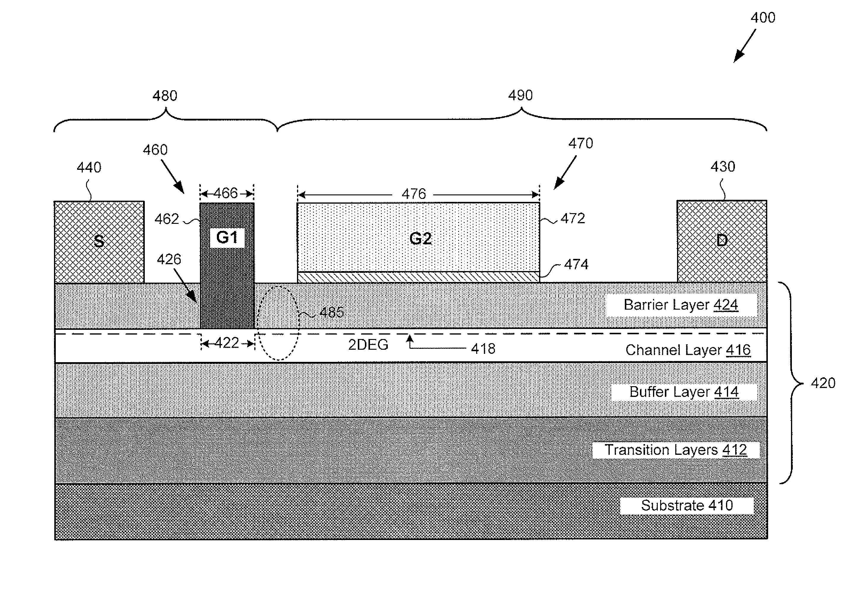
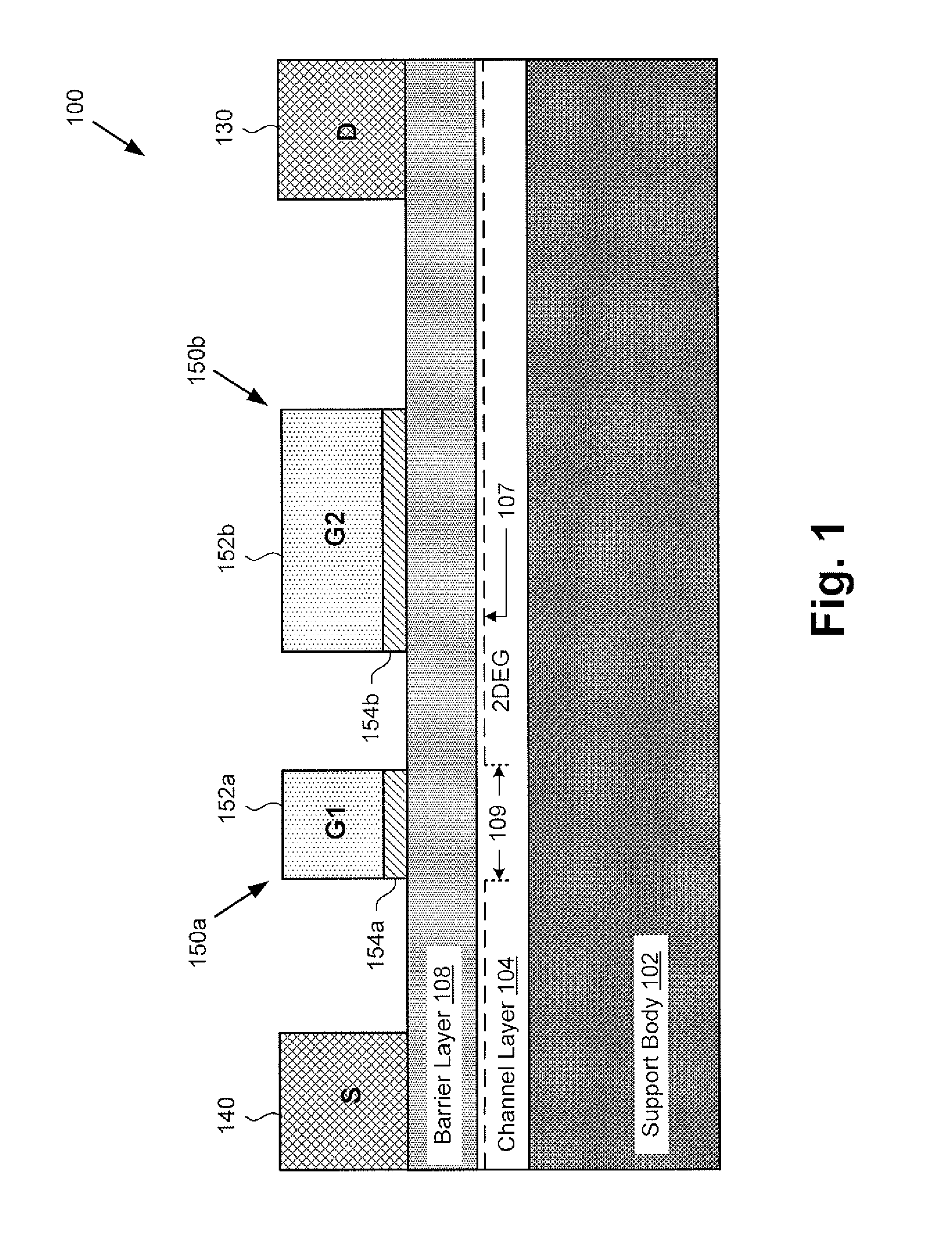
[0016]FIG. 1 shows a cross-sectional view of a dual gated merged III-Nitride transistor according to a conventional implementation. Dual gated merged transistor 100 includes support body 102, channel layer 104, barrier layer 108 overlying channel layer 104, drain electrode 130, source electrode 140,...


PUM


Abstract

There are disclosed herein various implementations of a group III-V merged cascode transistor. Such a group III-V merged cascode transistor includes a group III-V body disposed over a substrate and configured to produce a two-dimensional electron gas (2DEG). The group III-V body includes a group III-V barrier layer situated over a group III-V channel layer, and a source electrode and a drain electrode. The group III-V merged cascode transistor also includes an enable gate disposed in a recess extending substantially through the group III-V barrier layer, and an operational gate disposed over the group III-V barrier layer, the operational gate not being in physical contact with the enable gate.

Description

[0001]The present application claims the benefit of and priority to a provisional application entitled “Dual Gated Merged Cascode Device,” Ser. No. 61 / 913,156 filed on Dec. 6, 2013. The disclosure in this provisional application is hereby incorporated fully by reference into the present application.BACKGROUND[0002]I. Definition[0003]As used herein, the phrase “group III-V” refers to a compound semiconductor including at least one group III element and at least one group V element. By way of example, a group III-V semiconductor may take the form of a III-Nitride semiconductor. “III-Nitride” or “III-N” refers to a compound semiconductor that includes nitrogen and at least one group III element such as aluminum (Al), gallium (Ga), indium (In), and boron (B), and including but not limited to any of its alloys, such as aluminum gallium nitride (AlxGa(1-x)N), indium gallium nitride (InyGa(1-y)N), aluminum indium gallium nitride (AlxInyGa(1-x-y)N), gallium arsenide phosphide nitride (GaAsa...

Claims


Application Information

Patent Timeline
Patent Type & Authority Applications(United States)
IPC IPC(8): H01L29/778
CPCH01L29/778H01L29/42316H01L29/4236H01L29/7786H01L29/7831H01L29/7832H01L29/2003
Inventor BRIERE, MICHAEL A.
Owner INFINEON TECH AMERICAS CORP
Why Eureka
Try Eureka