
Liquid Crystal Display Touch Screen Array Substrate and the Corresponding Liquid Crystal Display Touch Screen

a liquid crystal display and touch screen technology, applied in the field of thin film transistor liquid crystal display, can solve the problems of increasing the power consumption of increasing the difficulty of preparing the liquid crystal display touch screen, and increasing the opening ratio of the pixel, so as to reduce the processing number, reduce the density of lines, and increase the opening ratio of pixels.

Active Publication Date: 2015-07-02
TCL CHINA STAR OPTOELECTRONICS TECH CO LTD
View PDF29 Cites 12 Cited by
  • Summary
  • Abstract
  • Description
  • Claims
  • Application Information

AI Technical Summary

Benefits of technology

The present invention relates to a liquid crystal display touch screen array substrate and corresponding liquid crystal display touch screen, which can reduce power consumption, simplify the process, and improve product yield. The technical effects of the patent include reducing line arranged density and increasing opening ratio in pixels, decreasing processing number, simplifying process, and enhancing sensitivity of touch position. Additionally, a synchronous second-order driving signal is utilized to reduce power consumption and improve display quality.

Problems solved by technology

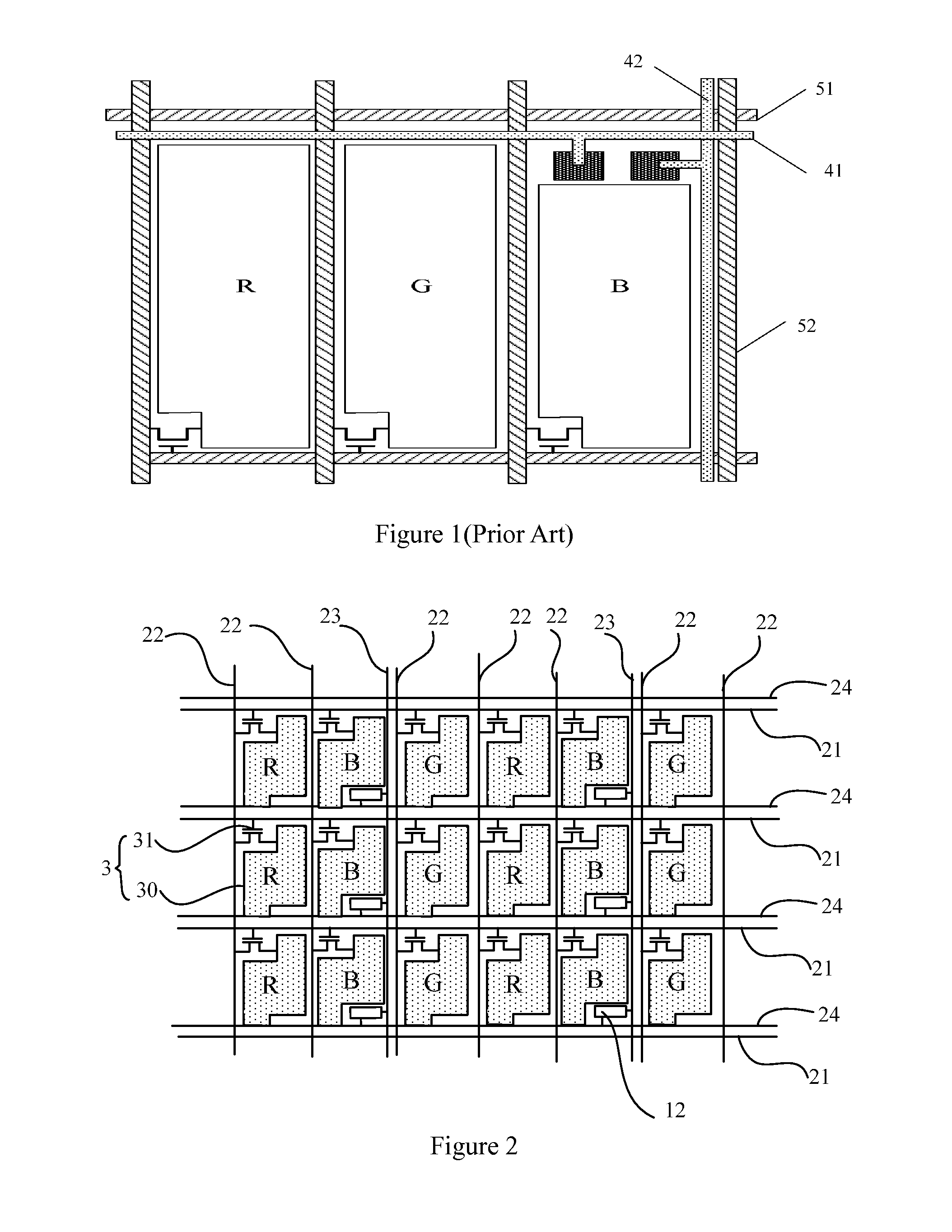
Therefore, when the gate line 51 and the data line 52 used to display intersect with the touch emission line 41 and the touch sensing line 42 used for touch function, it can not only decrease the opening ratio of the pixel, but also increase the process difficulty for preparing liquid crystal display touch screen, and then the bad operation will increase correspondingly.
Moreover, the touch emission line 41 needs independent driving signal, which will further increase the power consumption of the liquid crystal display touch screen.

Method used


Image

  • Liquid Crystal Display Touch Screen Array Substrate and the Corresponding Liquid Crystal Display Touch Screen
  • Liquid Crystal Display Touch Screen Array Substrate and the Corresponding Liquid Crystal Display Touch Screen
  • Liquid Crystal Display Touch Screen Array Substrate and the Corresponding Liquid Crystal Display Touch Screen

Examples


Embodiment Construction

[0049]The following description of the embodiments with reference to the attached drawings, the present invention may be used to illustrate the specific embodiments to implement. The present invention mentioned directional terms, such as “upper”, “lower”, “front”, “rear”, “Left”, “Right”, “top”, “bottom”, “horizontal”, “vertical”, etc. only with reference to the accompanying drawings, in the direction. Therefore, the use of directional terms are used to describe and understand the present invention and not intended to limit the present invention.

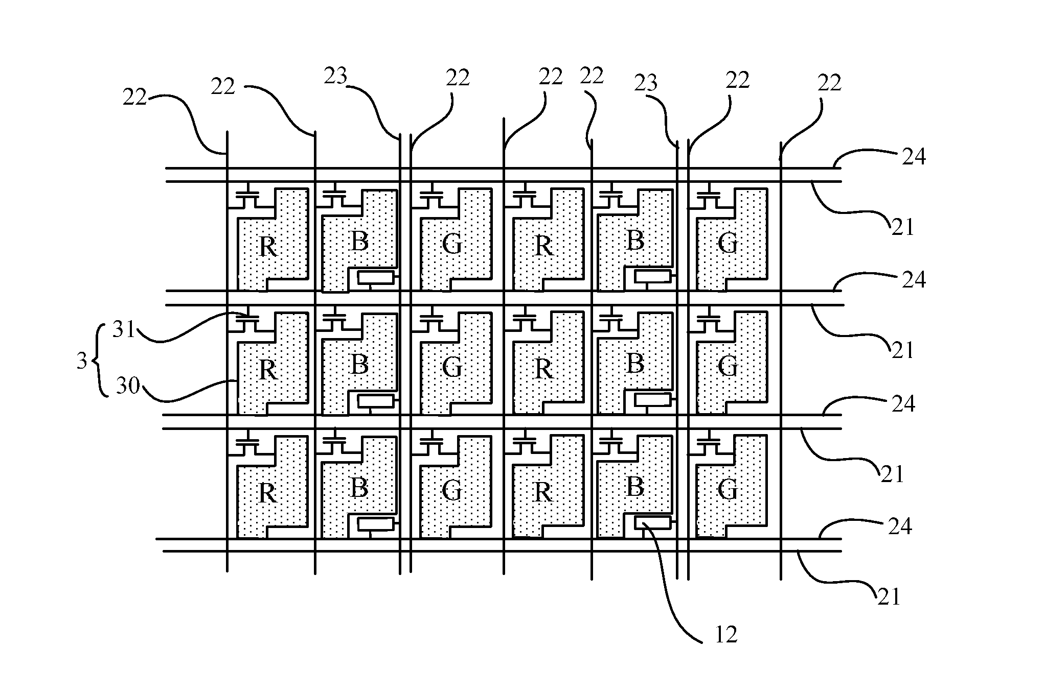
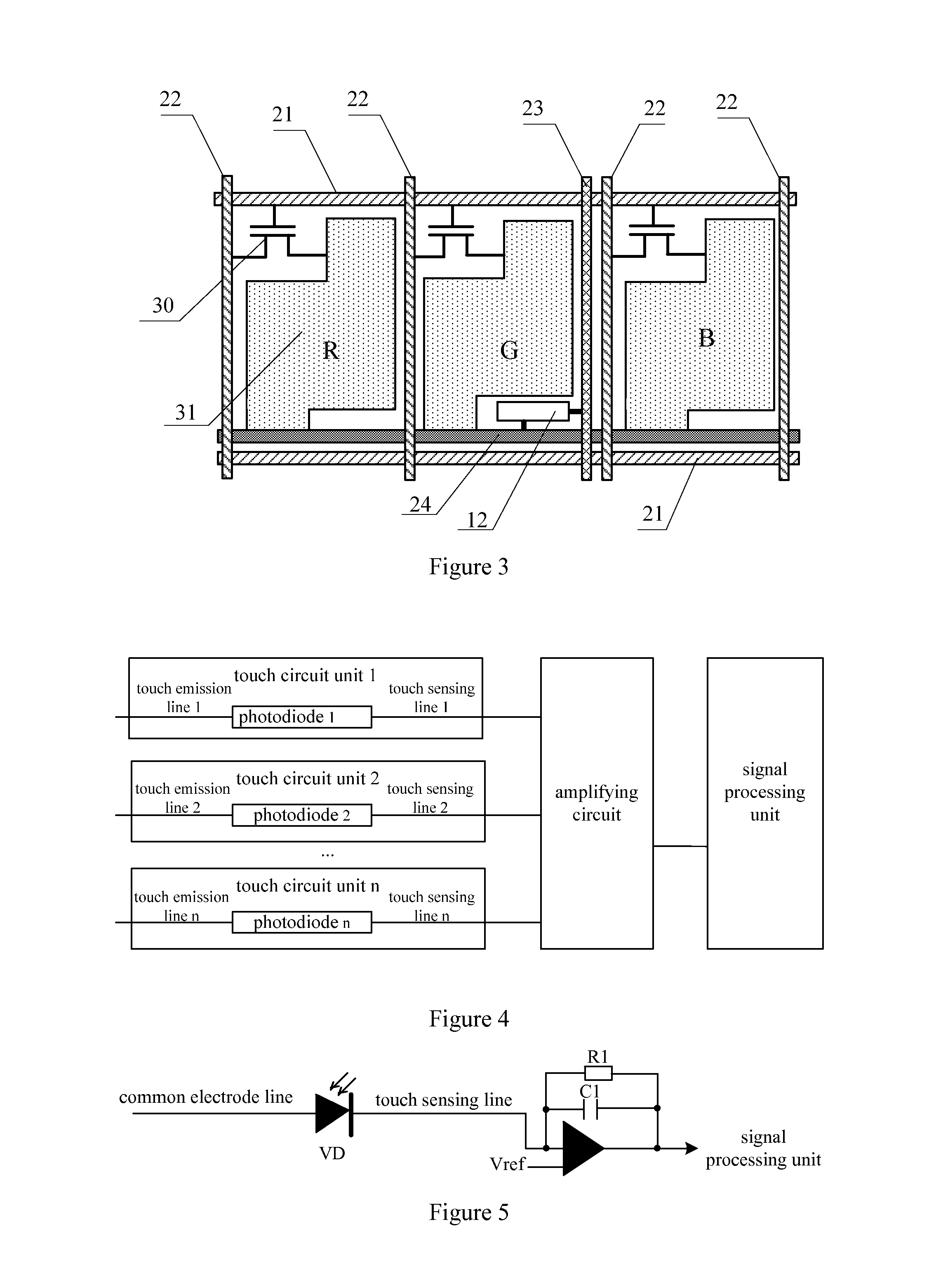
[0050]Referring to FIGS. 2 and 3, it shows a liquid crystal display touch screen array substrate according to an embodiment of the present invention. In the embodiment, the liquid crystal display touch screen array substrate comprises multiple pixel units 3 defined by multiple gate lines 21 and multiple data lines 22. Each pixel unit 3 is provided with a thin film transistor 30 and a pixel electrode 31 inside. The thin film transistor 30 is ...


PUM


Abstract

The present invention discloses a liquid crystal display touch screen array substrate, which comprises multiple pixel units defined by a gate line and a data line, each pixel unit is provided with a thin film transistor and a pixel electrode inside; a common electrode line provided in parallel at the side of each said gate line; which further comprise: a touch circuit unit used for touch positioning, the touch circuit unit comprising a touch emission line and a touch sensing line intersecting each other, and a light sensing unit provided at the intersection and respectively connected to the touch emission line and the touch sensing line. The touch emission line is the common electrode line, and the touch sensing line is parallel with the data line. The embodiment of the present invention correspondingly discloses a liquid crystal display touch screen. According to the embodiment of the present invention, it can enhance the sensitivity of the touch position, reduce the power consumption of the touch display screen, and improve the product yield.

Description

CROSS REFERENCE [0001]This application is claiming a priority arisen from a patent application, entitled with “Liquid Crystal Display Touch Screen Array Substrate and the Corresponding Liquid Crystal Display Touch Screen”, submitted to China Patent Office on Dec. 26, 2013, designated with an Application Number 201310730048.3. The whole and complete disclosure of such patent application is hereby incorporated by reference. This application also related to National Stage Application No.:______ (Attorney Docket No. CP14013), submitted on the same date, entitled, “Liquid Crystal Display Touch Screen Array Substrate and the Corresponding Liquid Crystal Display Touch Screen”; National Stage Application No.:______ (Attorney Docket No. CP14014), submitted on the same date, entitled, “Embedded Touch Array Substrate and Liquid Crystal Display Panel”; National Stage Application No.:______ (Attorney Docket No. CP14015), submitted on the same date, entitled, “Array Substrate Common Electrode Str...

Claims


Application Information

Patent Timeline
Patent Type & Authority Applications(United States)
IPC IPC(8): G06F3/041
CPCG06F3/0412G02F1/13338G02F1/13318G06F3/04166G06F3/042G06F3/04164G09G3/3655G09G5/18G09G2330/021
Inventor XU, XIANGYANG
Owner TCL CHINA STAR OPTOELECTRONICS TECH CO LTD
Learn More