Semiconductor package, fabrication method therefor, and package-on package

a technology of semiconductor and assembly, which is applied in the field of semiconductor package, can solve the problems of difficult to precisely form through holes and various process defects in conventional art, and achieve the effects of reducing damage, low process defects, and having precision

Active Publication Date: 2015-07-02
NEPES CO LTD
View PDF4 Cites 89 Cited by
  • Summary
  • Abstract
  • Description
  • Claims
  • Application Information

AI Technical Summary

Benefits of technology

[0047]Unlike a conventional art installing a semiconductor chip, forming a through hole, filling the through hole, and forming a through wiring, since the semiconductor package according to the spirit of the present invention previously forms the through hole in an insulating substrate, forms the through wiring by filling the through hole, and installs the semiconductor chip, the through wiring capable of reducing damage with respect to the semiconductor chip during a manufacturing process and having precision and a low process defect can be provided.
[0048]Further, since a protective layer is formed on an activation surface of the semiconductor chip, defects occurred in the processing of the activation surface of the semiconductor chip in an individualization process of the semiconductor chip, an installation process and a molding process on a carrier substrate, for example, defects such as damage of the activation surface of the semiconductor chip, contamination of pads of the semiconductor chip, coverage of a pad surface of a molding member, etc. can be prevented.
[0049]Moreover, since a semiconductor chip pad of the semiconductor chip is formed in a different plane from a lower pad connected to the through wiring by the protective layer, signal interference can be suppressed. A height of the lower pad can be adjusted by controlling a thickness of an insulating layer located on the semiconductor chip and insulating substrate, and electrical and mechanical characteristics of the semiconductor package can be controlled.

Problems solved by technology

However, the conventional art generates various process defects due to damage of a surface of a chip pad or penetration of a molding material, etc. during a manufacturing process.
Further, the conventional art has limitations that it is difficult to precisely form the through hole for forming the through pattern which is formed in the molding region of the semiconductor chip and densely fill the through hole with a conductive material.

Method used


Image

  • Semiconductor package, fabrication method therefor, and package-on package
  • Semiconductor package, fabrication method therefor, and package-on package
  • Semiconductor package, fabrication method therefor, and package-on package

Examples


Embodiment Construction

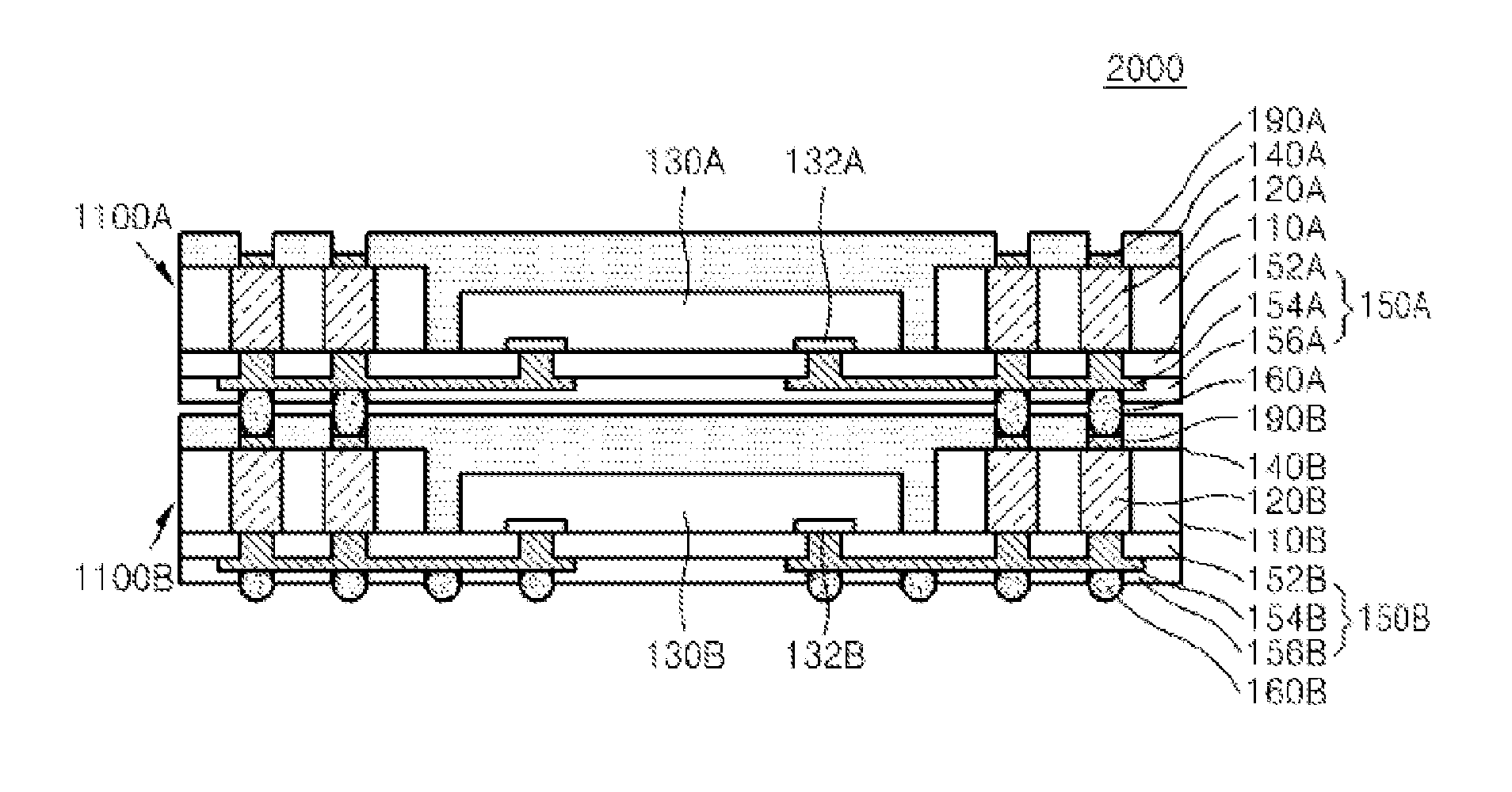
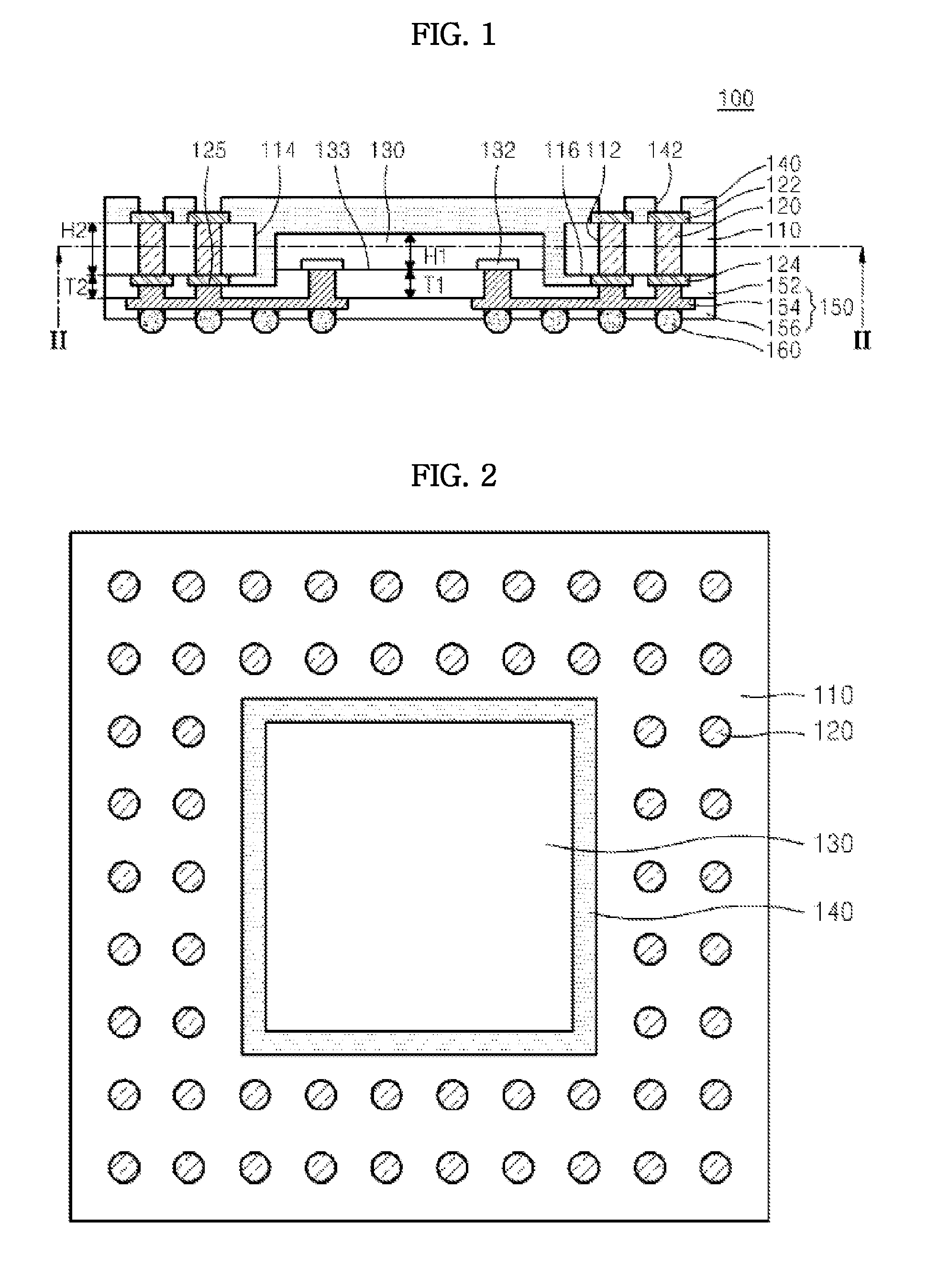
[0064]The semiconductor package according to an embodiment of the present invention includes an insulating substrate 110 including a first through portion 112 and a second through portion 114; a through wiring 120 which fills the first through portion 112, and is located to penetrate the insulating substrate 110; a semiconductor chip 130 which is located in the second through portion 114, and is electrically connected to the through wiring 120; a molding member 140 molding the semiconductor chip 130 and the insulating substrate 110; and a re-wiring pattern layer 150 which is located at a lower side of the insulating substrate 110, and electrically connects the through wiring 120 and the semiconductor chip 130.

[0065]Hereinafter, preferred embodiments of the present invention will be described with reference to accompanying drawings. Embodiments of the present invention are provided to describe more fully the spirit of the present invention to those skilled in the art, but the spirit ...


PUM


Abstract

Provided is a method of manufacturing a semiconductor package including a through wiring having precision and a low process defect. The semiconductor package includes an insulating substrate including a first through portion and a second through portion; a through wiring which fills the first through portion, and is located to penetrate the insulating substrate; a semiconductor chip which is located in the second through portion, and is electrically connected to the through wiring; a molding member molding the semiconductor chip and the insulating substrate; and a re-wiring pattern layer which is located at a lower side of the insulating substrate, and electrically connects the through wiring and the semiconductor chip.

Description

TECHNICAL FIELD[0001]The following description relates to a semiconductor package, and more particularly, to a semiconductor package including a through wiring, a method of manufacturing the same, and a package on package (PoP).BACKGROUND ART[0002]With continuous developments of a process of manufacturing a semiconductor chip, a size of the semiconductor chip has continuously decreased. Currently, since the size of the semiconductor chip is greatly decreased, when forming a semiconductor package, it is necessary to increase a size of the semiconductor package for electrical connection. One of semiconductor package technologies proposed in the process of the developments is a fan-out package. Further, technology expanding a memory capacity or improving operating performance of a semiconductor chip in the same installation dimension by forming a pattern structure transferring a signal in a vertical direction in an outer region of the fan-out package and stacking packages of the same k...

Claims


Application Information

Patent Timeline
Patent Type & Authority Applications(United States)
IPC IPC(8): H01L25/10H01L23/00H01L25/065H01L21/56H01L23/31H01L23/498
CPCH01L25/105H01L2225/107H01L23/49827H01L25/0655H01L21/56H01L24/89H01L24/08H01L24/83H01L24/32H01L2225/06548H01L2225/06572H01L2224/08111H01L2224/08235H01L2224/32235H01L23/3107H01L21/568H01L23/5389H01L24/19H01L24/24H01L24/82H01L2224/0401H01L2224/04105H01L2224/12105H01L2224/24101H01L2224/24155H01L2225/1035H01L2225/1041H01L2225/1058H01L2924/12042H01L2924/171H01L2924/181H01L2924/18162H01L2924/00
Inventor KWON, YONG-TAEPARK, KYUNG-HOON
Owner NEPES CO LTD
Why Eureka
Try Eureka