Liquid crystal display device and manufacturing method thereof

a liquid crystal display and horizontal inplane switching technology, applied in non-linear optics, instruments, optics, etc., can solve the problems of increased manufacturing costs and inefficient manufacturing processes of conventional ah-ips type lcds, and achieve the effect of reducing manufacturing processes and costs

Active Publication Date: 2015-07-02
LG DISPLAY CO LTD
View PDF10 Cites 10 Cited by
  • Summary
  • Abstract
  • Description
  • Claims
  • Application Information

AI Technical Summary

Benefits of technology

[0018]An advantage of the present invention is to provide an LCD that can reduce manufacturing processes and costs.
[0019]Additional features and advantages of the invention will be set forth in the description which follows, and in part will be apparent from the description, or may be learned by practice of the invention. These and other advantages of the invention will be realized and attained by the structure particularly pointed out in the written description and claims hereof as well as the appended drawings.
[0020]To achieve these and other advantages and in accordance with the purpose of the present invention, as embodied and broadly described herein, a liquid crystal display device includes a gate electrode; a gate insulating layer on the gate electrode; an active layer on the gate insulating layer corresponding to the gate electrode; source and drain electrodes on the active layer; a first passivation layer on the source and drain electrodes; a common electrode on the first passivation layer; a second passivation layer on the common electrode, covering the common electrode, and having a separate region from the first passivation layer at a thickness of the common electrode; a pixel electrode on the second passivation layer and connected to the drain electrode through a drain contact hole; and a common line at a same layer as the pixel electrode and connected to the common electrode.
[0021]In another aspect, a liquid crystal display device includes a gate electrode; a gate insulating layer on the gate electrode; an active layer on the gate insulating layer corresponding to the gate electrode; source and drain electrodes on the active layer; a first passivation layer on the source and drain electrodes; a second passivation layer on the first passivation layer; a common electrode on the second passivation layer and exposing a portion of the second passivation layer; a third passivation layer on the common electrode and having a separate region from the second passivation layer, wherein the common electrode is not located at the separate region; a pixel electrode on the third passivation layer and connected to the drain electrode through a drain contact hole; and a common line at a same layer as the pixel electrode and connected to the common electrode.
[0022]In another aspect, a method of manufacturing a liquid crystal display device includes forming a gate line, a gate electrode and a gate pad on a substrate; forming a gate insulating layer on the gate line, the gate electrode and the gate pad; forming a data line, a source electrode, a drain electrode and a data pad on the gate insulating layer; forming a first passivation layer on the data line, the source electrode, the drain electrode and the data pad; forming a common layer on the first passivation layer; forming a second passivation layer on the common layer; first dry etching the second passivation layer; first wet etching the common layer exposed through the first dry-etched second passivation layer to form a common pattern; second dry etching the gate insulating layer, the first passivation layer and the second passivation layer; second wet etching the common pattern exposed through the second dry-etched second passivation layer to form a common electrode; and forming a pixel electrode and a common line on the second passivation layer.
[0023]It is to be understood that both the foregoing general description and the following detailed description are exemplary and explanatory and are intended to provide further explanation of the invention as claimed.

Problems solved by technology

Therefore, manufacturing processes of conventional AH-IPS type LCDs are inefficient and manufacturing costs are increased.

Method used


Image

  • Liquid crystal display device and manufacturing method thereof
  • Liquid crystal display device and manufacturing method thereof
  • Liquid crystal display device and manufacturing method thereof

Examples


Embodiment Construction

[0028]Reference will now be made in detail to exemplary embodiments, examples of which are illustrated in the accompanying drawings. The same reference numbers may be used throughout the drawings to refer to the same or like parts.

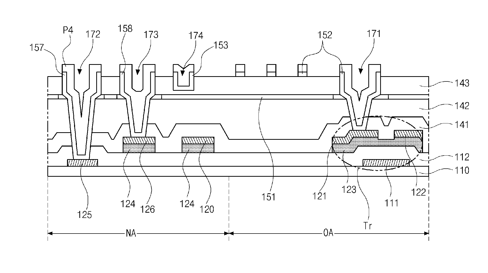
[0029]FIG. 2 is a cross-sectional view illustrating an AH-IPS type LCD according to an embodiment of the present invention.

[0030]Referring to FIG. 2, the LCD includes an array substrate including a display region OA to display an image and a non-display region NA. The display region OA corresponds to a pixel region.

[0031]In the array substrate, a gate electrode 111 is formed in the pixel region on a substrate 110, a gate insulating layer 112 is formed on the gate electrode 111, and an active layer 123 is formed on the gate insulating layer 112. A source electrode 122 and a drain electrode 121 are formed on the active layer 123 and spaced apart from each other. First and second passivation layers 141 and 142 are formed on the source and drain electrodes 122...


PUM


Abstract

A liquid crystal display device includes a gate electrode; a gate insulating layer on the gate electrode; an active layer on the gate insulating layer corresponding to the gate electrode; source and drain electrodes on the active layer; a first passivation layer on the source and drain electrodes; a common electrode on the first passivation layer; a second passivation layer on the common electrode, covering the common electrode, and having a separate region from the first passivation layer at a thickness of the common electrode; a pixel electrode on the second passivation layer and connected to the drain electrode through a drain contact hole; and a common line at a same layer as the pixel electrode and connected to the common electrode.

Description

CROSS-REFERENCE TO RELATED APPLICATION[0001]This application claims the benefit of Korean Patent Application No. 10-2013-0169083, filed on Dec. 31, 2013, which is hereby incorporated by reference for all purposes as if fully set forth herein.BACKGROUND OF THE INVENTION[0002]1. Field of the Invention[0003]The present disclosure relates to an advanced horizontal in-plane switching (AH-IPS) type liquid crystal display device (LCD) and a manufacturing method thereof.[0004]2. Discussion of the Related Art[0005]An LCD displays images using a liquid crystal panel and a backlight unit.[0006]Conventionally, a twisted nematic (TN) type LCD is used. Alternatively, vertical alignment (VA) type and in-plane switching (IPS) type LCDs are widely used.[0007]Recently, an AH-IPS type LCD is developed. The AH-IPS type LCD provides a better viewing angle and contrast ratio than the IPS type LCD.[0008]Figure (FIG. 1 is a cross-sectional view illustrating an AH-IPS type LCD according to related art.[0009...

Claims


Application Information

Patent Timeline
Patent Type & Authority Applications(United States)
IPC IPC(8): H01L27/12H01L29/66H01L29/786
CPCH01L27/1214H01L27/1259H01L29/66742H01L29/786G02F1/136227G02F1/134372H01L27/124H01L27/1288G02F1/136G02F1/1368
Inventor KIM, YONG-ILKIM, MIN-JOO
Owner LG DISPLAY CO LTD
Why Eureka
Try Eureka