Method for fabricating semiconductor device

a technology of semiconductor devices and fabrication methods, applied in the direction of semiconductor devices, basic electric elements, electrical equipment, etc., can solve the problems of weakening or removing desired stress, overfilling, and adverse effects on the device performance of the resultant cmos devices

Active Publication Date: 2015-07-02
SEMICON MFG INT (SHANGHAI) CORP
View PDF12 Cites 229 Cited by
  • Summary
  • Abstract
  • Description
  • Claims
  • Application Information

AI Technical Summary

Problems solved by technology

However, overfill may occur to the stress layers to have a top surface protruding above a top surface of the substrate,
Such overfill of the stress layers may generate uneven surface of the substrate and thus impede subsequent manufacturing processes In addition, overfill of the stress layers may affect stress distribution in the stress layers, e.g., may weaken or remove desired stress to be generated in the stress layers.
Device performance of the resultant CMOS devices may be adversely affected.
However, a single wafer may include a large amount of CMOS devices with different sizes.
Consequently, it is difficult to control the etch process of the overfill portions with different heights for various different CMOS devices on a same wafer.
For example, some stress layers of some CMOS devices may be etched to reach a desired height, e.g., to be substantially flat with the substrate surface, while other stress layers of other CMOS devices in the same wafer may be etched still having a height over / below the substrate surface due to unsufficient / over etching.

Method used


Image

  • Method for fabricating semiconductor device
  • Method for fabricating semiconductor device
  • Method for fabricating semiconductor device

Examples


Embodiment Construction

[0016]Reference will now be made in detail to exemplary embodiments of the disclosure, which are illustrated in the accompanying drawings. Wherever possible, the same reference numbers will be used throughout the drawings to refer to the same or like parts.

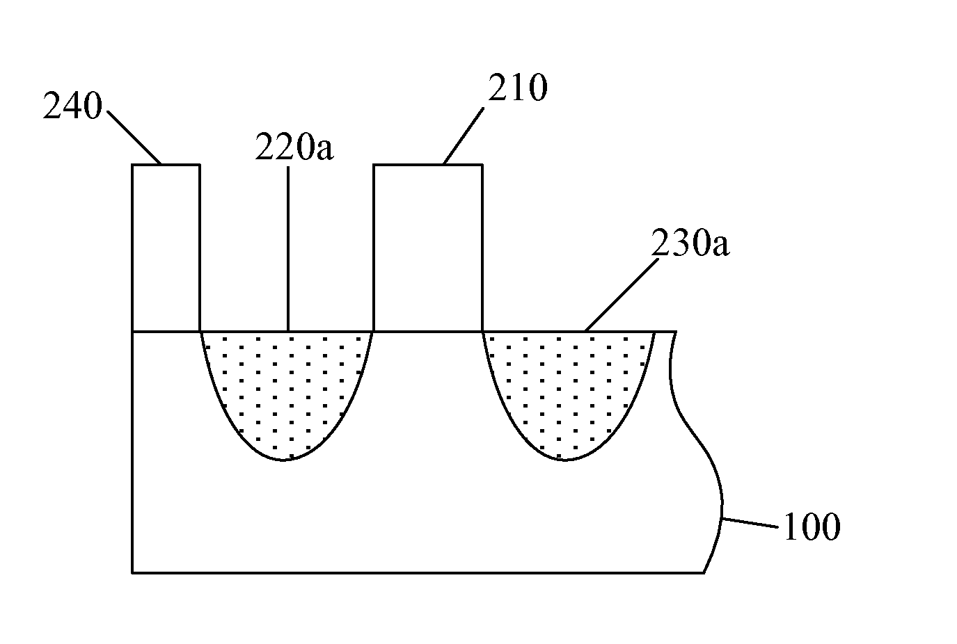
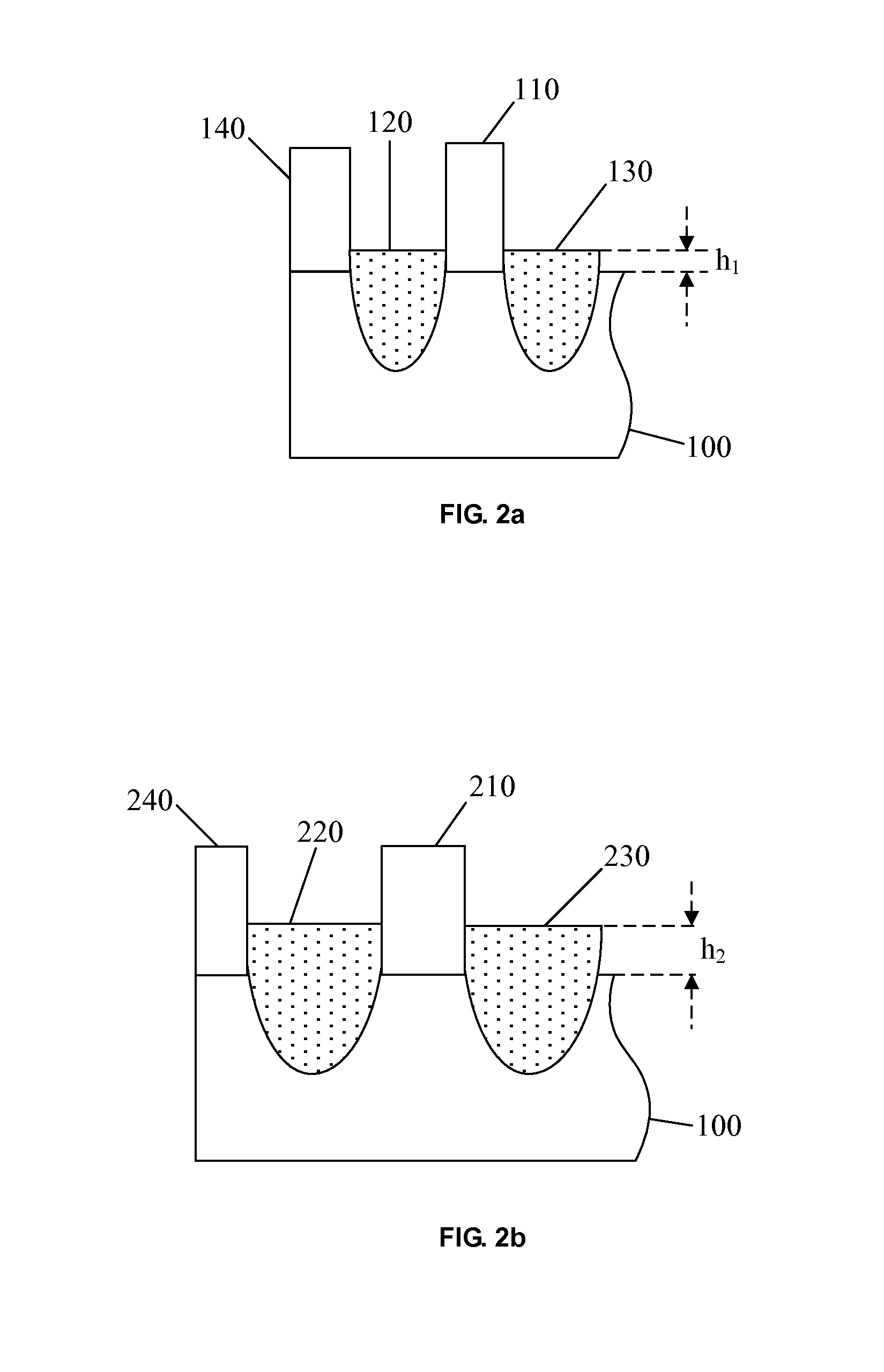
[0017]In a manufacturing process of a semiconductor device, source / drain regions can be formed by filling trenches in a substrate, which may generate overfills above a top surface of the substrate. As a result, source / drain regions in a same and / or different semiconductor device of a wafer may have different protruded heights over the substrate.

[0018]For forming CMOS devices, after forming source / drain regions, protruded portions of source / drain regions over the substrate can be removed by an etching process. However, due to various different sizes / pitches of trenches formed for CMOS devices on a same wafer, stress layers formed in these trenches can correspondingly have various etching areas with different sizes or pitches. Such ...


PUM


Abstract

Methods for fabricating semiconductor devices are provided. Gate structures are formed on a top surface of a substrate to form semiconductor devices. Trenches are formed in the substrate on both sides of each gate structure of each semiconductor device. The trenches on the both sides of each gate structure are filled with stress layers, the stress layers in the substrate protruding over the top surface of the substrate The stress layers are ion-doped and annealed on the both sides of each gate structure, and are pulse-etched to form a source region and a drain region of each gate structure. The pulse-etching is controlled such that the source regions and the drain regions of the plurality of semiconductor devices have a top surface coplanar with the top surface of the substrate.

Description

CROSS-REFERENCES TO RELATED APPLICATIONS[0001]This application claims priority to Chinese Patent Application No. CN201310745807.3, filed on Dec. 30, 2013, the entire content of which is incorporated herein by reference.FIELD OF THE DISCLOSURE[0002]The present disclosure relates to the field of semiconductor manufacturing technology and, more particularly, relates to semiconductor devices and fabrication methods.BACKGROUND[0003]When forming a CMOS device, a gate structure is often formed on a substrate, followed by forming trenches in the substrate on both sides of the gate structure. Stress layers are formed in the trenches and then are doped to form source / drain regions. However, overfill may occur to the stress layers to have a top surface protruding above a top surface of the substrate,[0004]Such overfill of the stress layers may generate uneven surface of the substrate and thus impede subsequent manufacturing processes In addition, overfill of the stress layers may affect stress...

Claims


Application Information

Patent Timeline
Patent Type & Authority Applications(United States)
IPC IPC(8): H01L29/66H01L21/02H01L29/78H01L21/3065
CPCH01L29/66477H01L21/3065H01L29/7848H01L21/02529H01L21/02532H01L21/02664H01L29/66636
Inventor ZHANG, HAIYANGREN, JIA
Owner SEMICON MFG INT (SHANGHAI) CORP
Why Eureka
Try Eureka