Organic electroluminescent device and organic electroluminescent display device

Active Publication Date: 2015-07-02
LG DISPLAY CO LTD
View PDF4 Cites 28 Cited by
  • Summary
  • Abstract
  • Description
  • Claims
  • Application Information

AI Technical Summary

Benefits of technology

[0011]An object of the present invention is to provide an organic electroluminesce

Problems solved by technology

In this regard, a blue emission layer has a lower efficiency than emission lay

Method used


Image

  • Organic electroluminescent device and organic electroluminescent display device
  • Organic electroluminescent device and organic electroluminescent display device
  • Organic electroluminescent device and organic electroluminescent display device

Examples


first embodiment

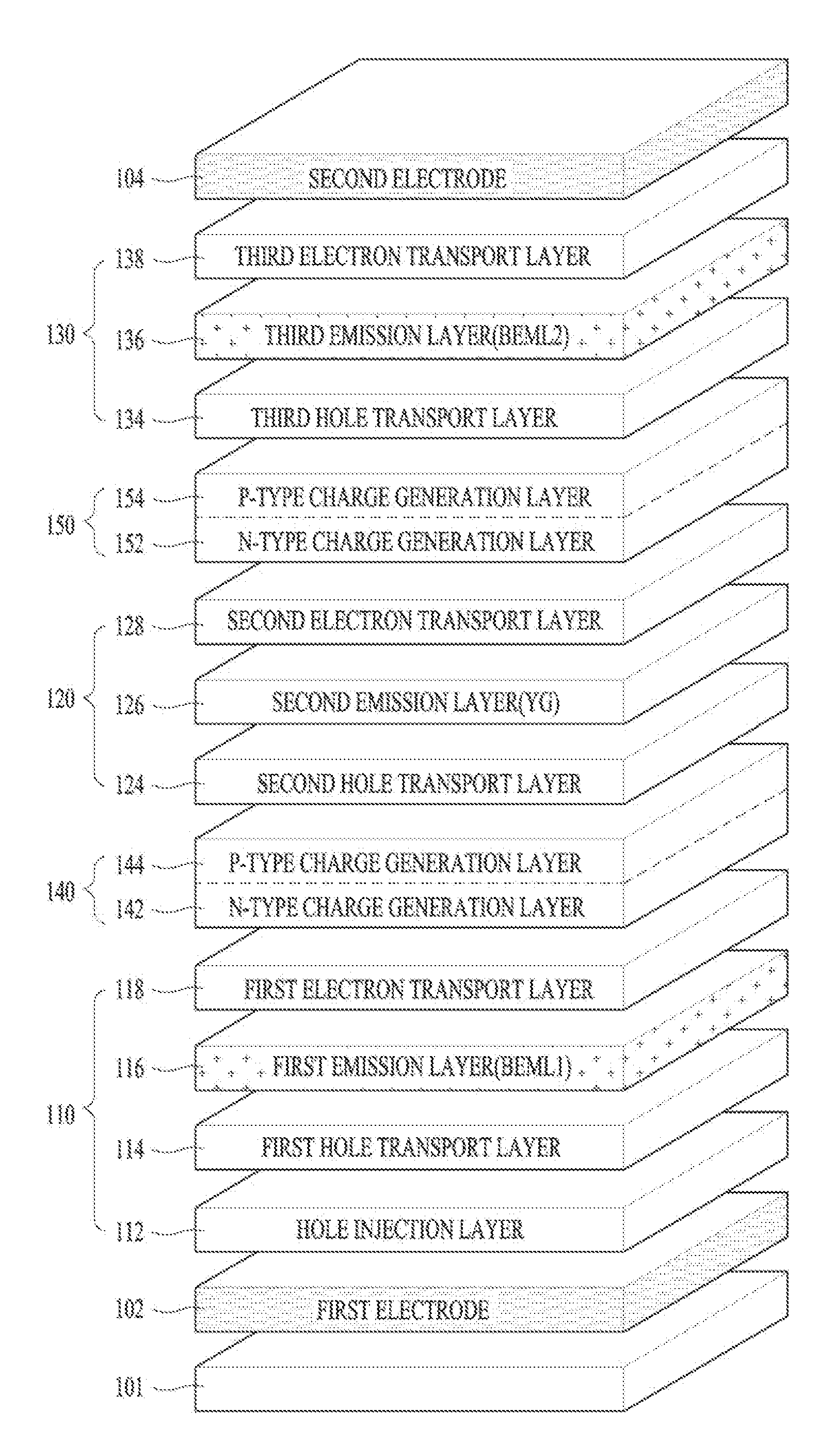
[0031]FIG. 1 is a perspective view of an organic electroluminescent device according to the present invention.

[0032]The organic electroluminescent device illustrated in FIG. 1 includes first and second electrodes 102 and 104 facing each other on a substrate 101, first, second and third light emitting units 110, 120 and 130 formed between the first and second electrodes 102 and 104, and first and second charge generation layers 140 and 150 respectively formed between the first and second light emitting units 110 and 120 and between the second and third light emitting units 120 and 130.

[0033]At least one of the first and second electrodes 102 and 104 is formed as a semi-transparent electrode. When the first electrode 102 is a semi-transparent electrode and the second electrode 104 is a reflective electrode, the organic electroluminescent device is of a bottom emission type that emits light to the lower side. When the second electrode 104 is a semi-transparent electrode and the first e...

second embodiment

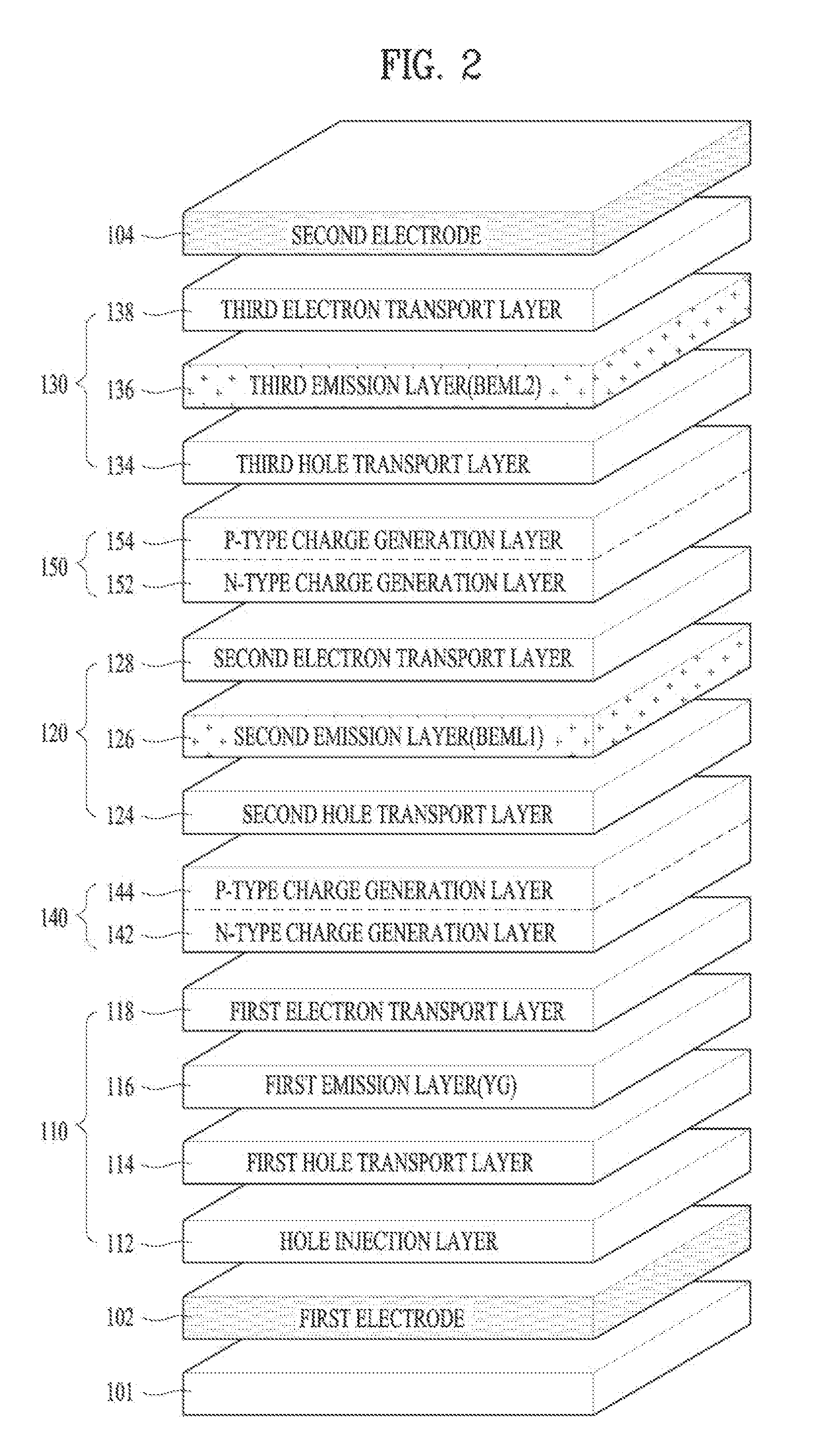
[0047]FIG. 5 is a sectional view of an organic electroluminescent device according to the present invention.

[0048]The organic electroluminescent device of FIG. 5 includes the same elements as those of the organic electroluminescent device of FIG. 1, except that emission layers are formed at specific positions. Thus, a detailed description of the same elements will be omitted herein.

[0049]The emission layers 116, 126 and 136 of the organic electroluminescent device according to the second embodiment of the present invention are arranged as illustrated in FIG. 5.

[0050]A separation distance T1 between the first blue emission layer BEML1, which is the first emission layer 116 close to the first electrode 102, and the second emission layer 126 that realizes yellow-green is less than a separation distance T2 between the second blue emission layer BEML2, which is the third emission layer 136 close to the second electrode 104, and the second emission layer 126 that realizes yellow-green. Fo...


PUM


Abstract

An organic electroluminescent device and organic electroluminescent display device having enhanced efficiency are discussed. In one example, the organic electroluminescent device includes first and second electrodes facing each other on a substrate and at least two emission layers formed between the first and second electrodes and realizing blue light, wherein, among the emission layers, a first blue emission layer close to the first electrode includes a first blue dopant having a different maximum luminescence wavelength than that of a second blue dopant of a second blue emission layer close to the second electrode.

Description

[0001]This application claims the benefit of Korean Patent Application No. 10-2013-0168049, filed on Dec. 31, 2013, which is hereby incorporated by reference as if fully set forth herein.BACKGROUND OF THE INVENTION[0002]1. Field of the Invention[0003]The present invention relates to an organic electroluminescent device and organic electroluminescent display device having enhanced efficiency.[0004]2. Discussion of the Related Art[0005]With the advent of the information era, the field of displays, which visually display electrical information signals, has rapidly developed. In line with such trend, a variety of ultra-thin and light flat display devices with low power consumption have been developed.[0006]Examples of such flat display devices include, but are not limited to, a liquid crystal display (LCD) device, a plasma display panel (PDP) device, a field emission display (FED) device, and an organic light emitting device (OLED).[0007]In particular, OLEDs are self-emissive and have f...

Claims


Application Information

Patent Timeline
IPC IPC(8): H01L51/50H01L27/32
CPCH01L51/5044H01L27/3244H01L27/3209H10K59/32H10K59/12H10K50/131H10K50/19H10K2102/351H10K50/13H10K50/11
Inventor AHN, SO-YEONHAN, CHANG-WOOKCHOI, HONG-SEOKJOUNG, SEUNG-RYONGCHO, GWI-JEONGCHOI, HEE-DONG
Owner LG DISPLAY CO LTD
Why Eureka
Try Eureka