

Pressing Force Sensor
- Summary
- Abstract
- Description
- Claims
- Application Information
AI Technical Summary
Benefits of technology
Problems solved by technology
Method used
Image

Examples
first embodiment
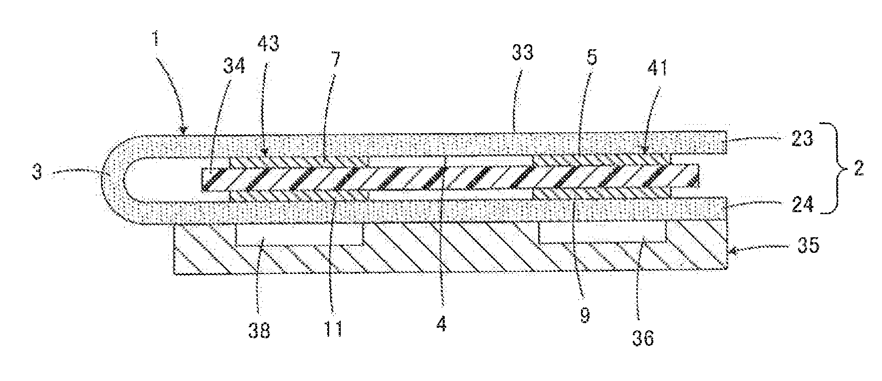
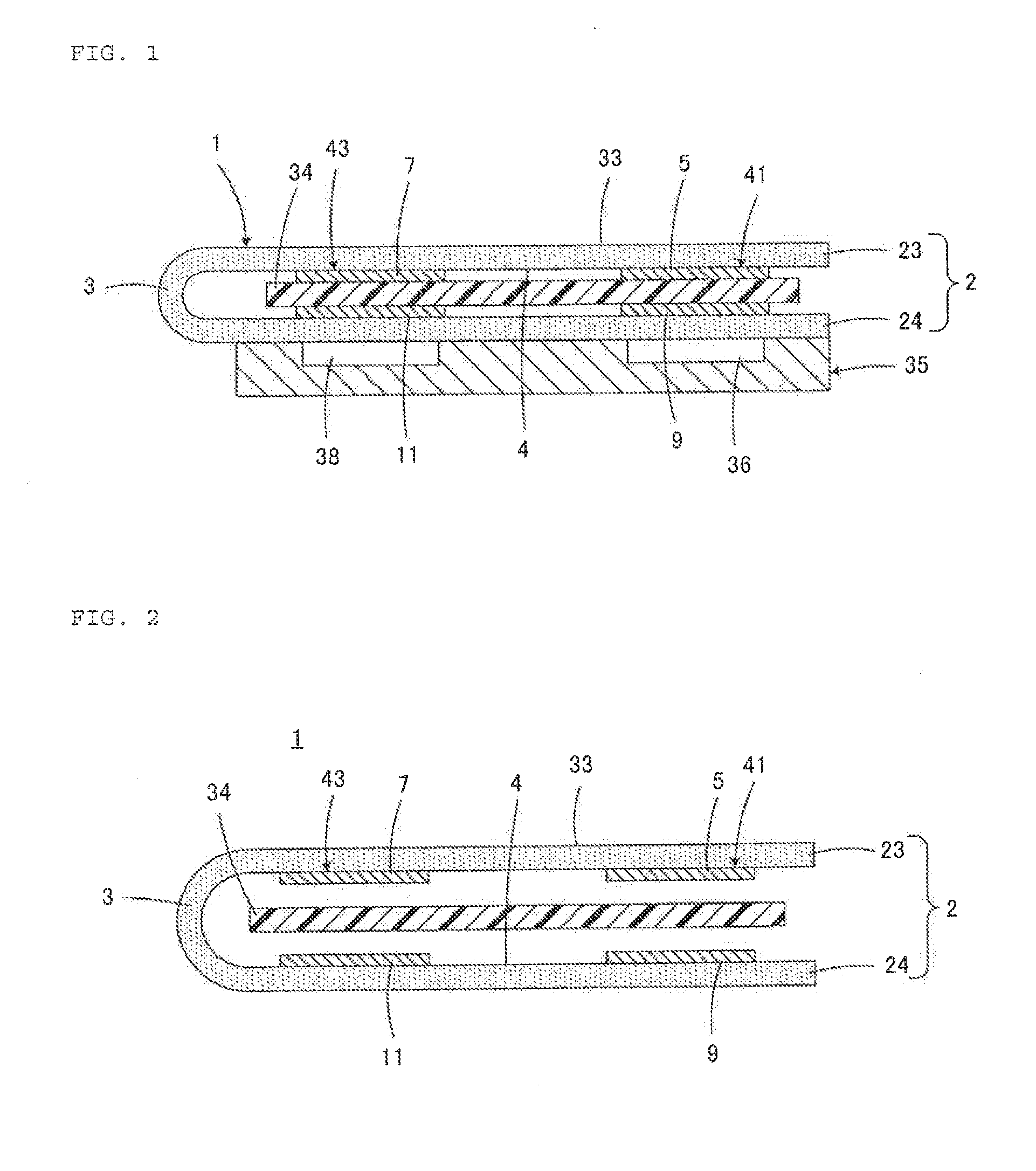
[0039]With reference to FIG. 1 to FIG. 6, a pressing force sensor 1 according to a first embodiment will be described. Note that, in FIG. 1 and FIG. 2, the dimensions in thickness directions of the components shown in the figures are exaggeratedly illustrated.
[0040]A pressing force sensor 1 is equipped with a flexible printed circuit board 2 having enough heat resistance to withstand solder reflow temperatures. Commercially available flexible printed circuit boards are made of, for example, polyimide and have enough heat resistance to withstand solder reflow temperatures. In the pressing force sensor 1, the flexible printed circuit board 2 is used while being folded via a predetermined folding line 3 as shown in FIG. 1 and FIG. 2.
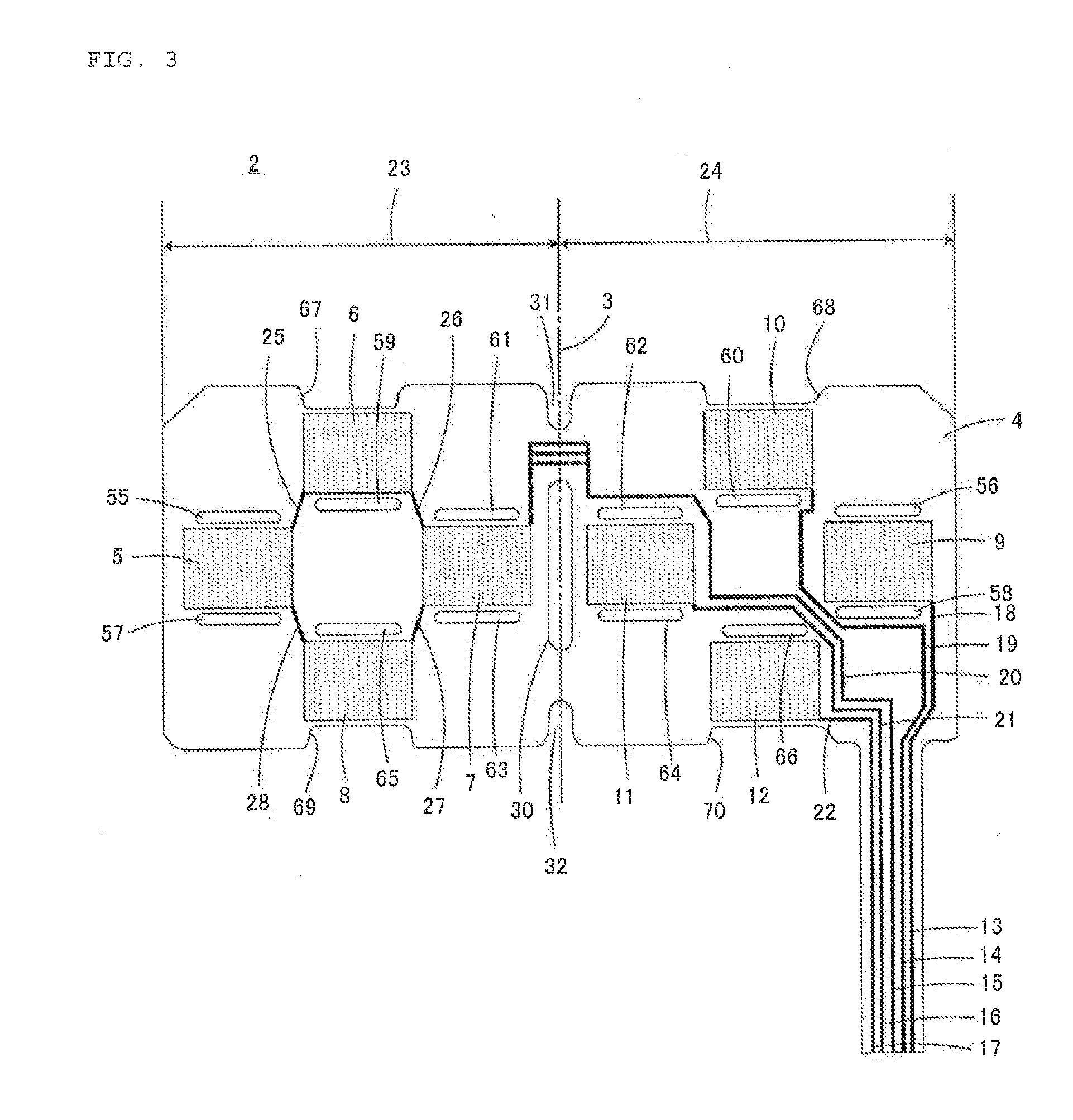
[0041]On a first principal surface 4 of the flexible printed circuit board 2, which faces inward when folded, there are formed, as well illustrated in FIG. 3, eight pressing force detection electrodes 5 to 12, five lead terminals 13 to 17 for connection to ...
second embodiment
[0061]With reference to FIG. 7, a pressing force sensor 1a according to a second embodiment will be described. FIG. 7 is a figure corresponding to FIG. 2. In FIG. 7, components corresponding to the components shown in FIG. 2 are assigned the same reference symbols, and will not be described again.
[0062]As can be understood from the comparison between FIG. 7 and FIG. 2, the pressing force sensor 1a shown in FIG. 7 is characterized in that the pressing force sensor 1a is further equipped with a shield electrode 73 formed on the second principal surface 33 of the flexible printed circuit board 2. This shield electrode 73 can function, for example, as a shield layer for electrostatic countermeasure when the shield electrode 73 is connected to the ground or the like.
[0063]In FIG. 7, the shield electrode 73 is formed on the flexible printed circuit board 2 except the folding line 3; however, the shield electrode 73 may be formed on the entire surface of the second principal surface 33 of ...
third embodiment
[0065]With reference to FIG. 8, a pressing force sensor 1b according to the third embodiment will be described. FIG. 8 is a figure corresponding to FIG. 2. In FIG. 8, components corresponding to the components shown in FIG. 2 are assigned the same reference symbols, and will not be described again.
[0066]The pressing force sensor 1b shown in FIG. 8 is characterized in that a sensor element is configured not with a piezoelectric film but with resistor films. FIG. 9 shows an example of an arrangement of the resistor films it a plan view.
[0067]With reference to FIG. 9, there are shown six resistor films 75 to 80 each having a meander shape. These resistor films 75 to 80 are formed by, for example, printing carbon paste. With reference to FIG. 9, various lines 81 connected to resistor films 75 to 80 represent electric wiring from the pressing force detection electrodes to the lead terminals. The resistor films 75 to 80 constitute a bridge circuit, where the resistor films 75, 76, 79, and...
PUM
 Abstract
Description
Claims
Application Information