Semiconductor Device

Active Publication Date: 2015-07-23
TOYOTA IND CORP
View PDF5 Cites 2 Cited by
  • Summary
  • Abstract
  • Description
  • Claims
  • Application Information

AI Technical Summary

Benefits of technology

The present invention provides a semiconductor element that can suppress the effect of current unbalance among semiconductor elements and can be downsized. The semiconductor element has an input electrode unit and an output electrode unit arranged in a specific region, which reduces the difference in current path length to each semiconductor element and minimizes the influence of current unbalance. The input electrode unit has a wider width in one direction, which ensures a sufficient connecting area to carry current, while a rectangular shape in the other direction maximizes the use of the third region to secure a sufficient connecting area. This allows for a smaller size of the semiconductor device.

Problems solved by technology

The prior art however has a problem as described below.
This results in large current unbalance among power elements.
Accordingly, when the current unbalance is large, it is required to increase the number of power elements to obtain a desired output current, which results in the requirement for a larger device.
Therefore, the timings of a current flowing into each semiconductor element are almost the same, and therefore the current unbalance among semiconductor elements is small.
However, since the electrode terminal and the output terminal extend in the direction along which the semiconductor elements are arrayed (the direction perpendicular to the direction along which the semiconductor element groups are arrayed), a large space for the electrode terminal and the output terminal are required.
Thus, the device becomes large.

Method used


Image

  • Semiconductor Device
  • Semiconductor Device
  • Semiconductor Device

Examples


Embodiment Construction

[0022]The embodiment of the present invention will be described in detail referring to the attached drawings. In the description, the same component or the component having the same function is denoted with the same reference sign and repeated description thereof will be omitted. Dimensional ratios in each drawing may be different from the actual dimensional ratios.

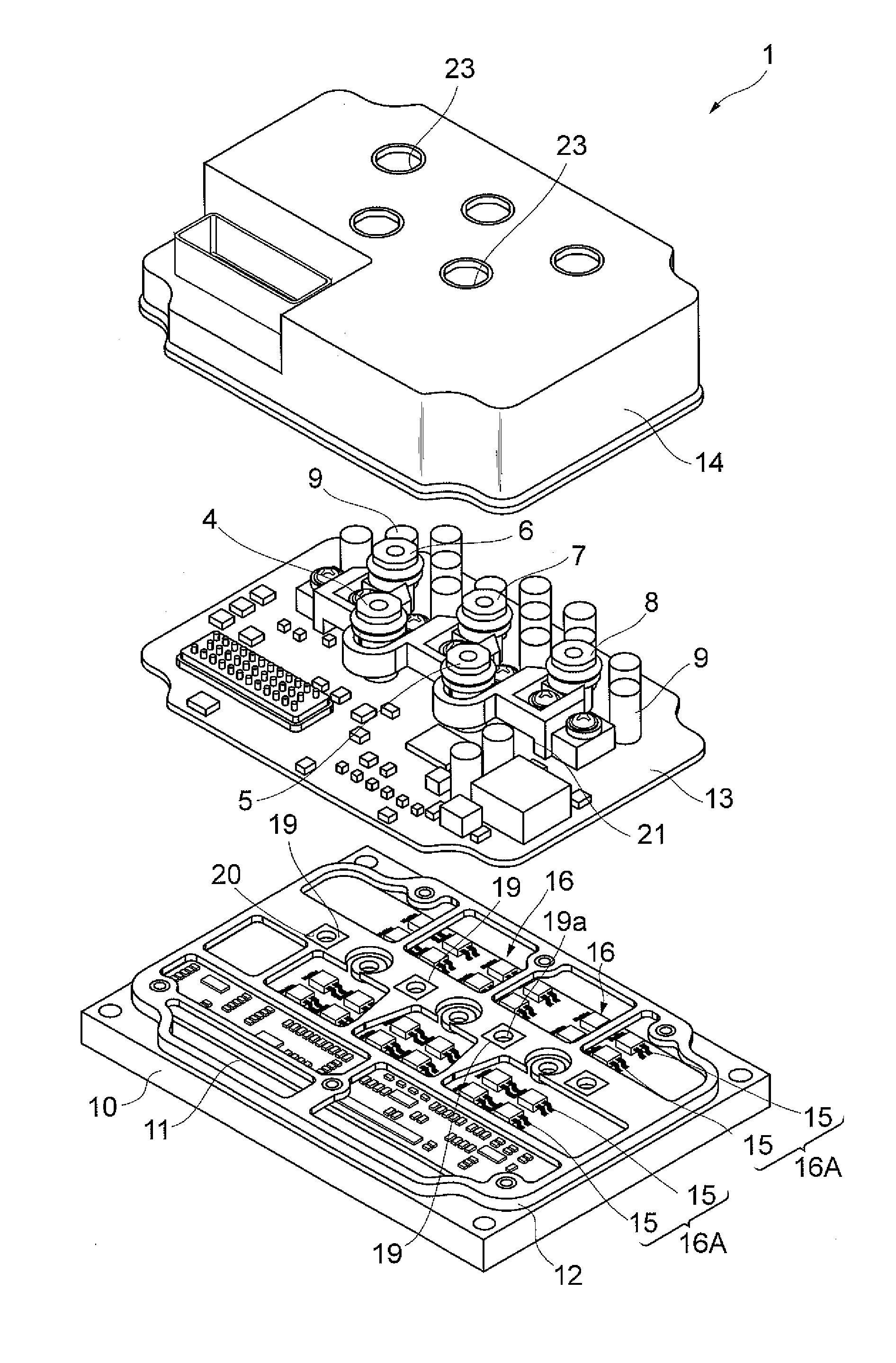
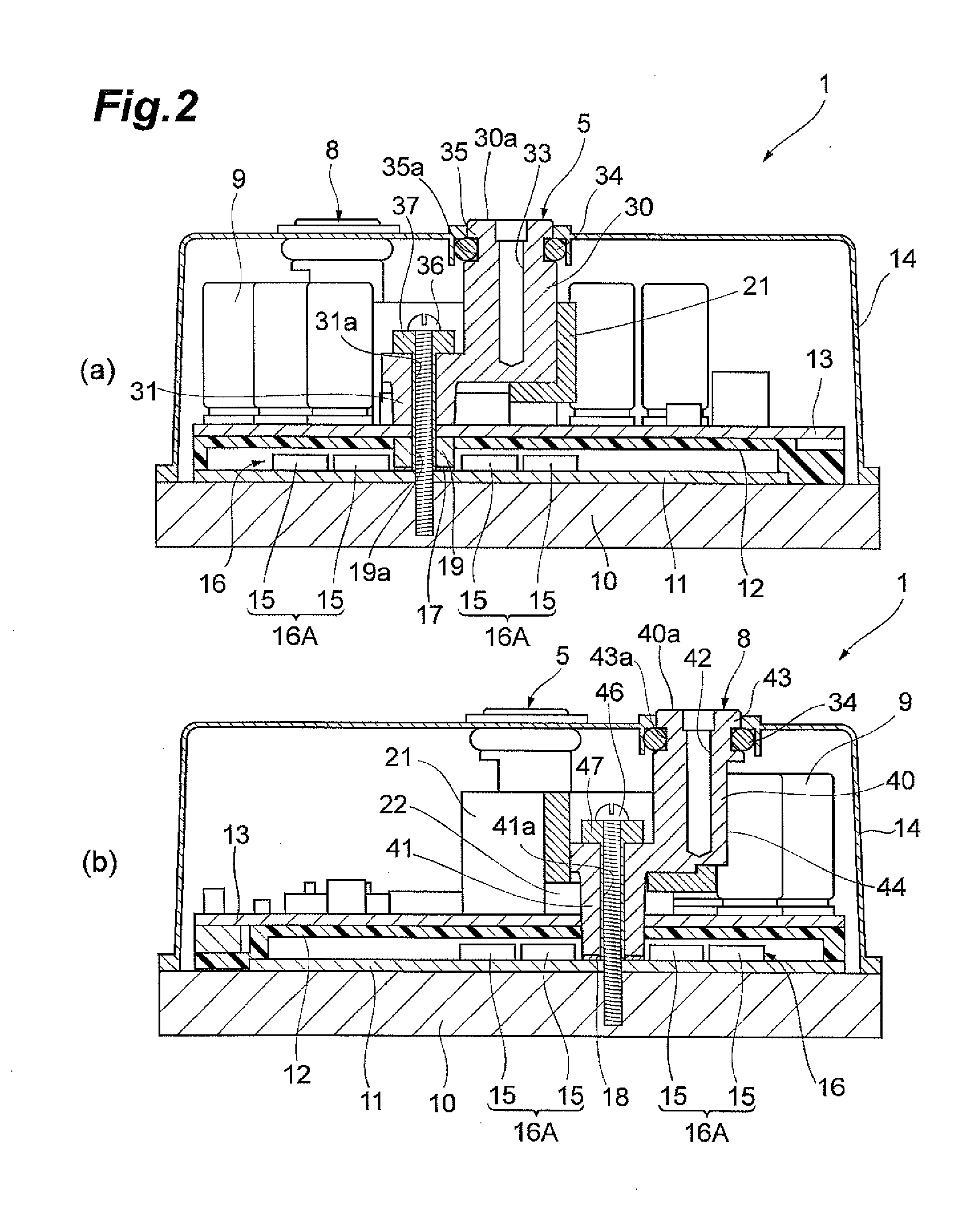
[0023]FIG. 1 is an exploded perspective view illustrating an inverter device according to the embodiment. FIG. 2 is sectional views of the inverter device illustrated in FIG. 1. In FIG. 2, (a) is a sectional view taken along the line IIA-IIA in FIG. 5 and (b) is a sectional view taken along the line IIB-IIB in FIG. 5. The inverter device 1 of the embodiment is, for example, a three-phase inverter device for driving a three-phase AC motor.

[0024]FIG. 3 is a circuit diagram of the inverter device 1. As illustrated in FIG. 3, the inverter device 1 includes a main circuit 2, a control circuit 3 for controlling the main circuit...


PUM


Abstract

A plurality of arm elements is arrayed along a first direction of a substrate. Each arm element includes a plurality of semiconductor elements connected in parallel. Each arm element is configured such that a plurality of semiconductor elements is arrayed along a second direction of the substrate which is perpendicular to the first direction and separated into a first element group and a second element group. The substrate includes a first region where the semiconductor element included in the first element group is arranged and a second region where the semiconductor element included in the second element group is arranged, and the first region and the second region are separated along the second direction. An input electrode unit and an output electrode unit are arranged along the first direction in a region provided between the first region and the second region on the substrate.

Description

BACKGROUND OF THE INVENTION[0001]1. Field of the Invention[0002]The present invention relates to a semiconductor device.[0003]2. Related Background Art[0004]As a conventional semiconductor device, for example, semiconductor devices discussed in U.S. Pat. No. 5,715,141 and JP Registered Utility Model Publication No. 3,173,512 are known. The semiconductor device discussed in U.S. Pat. No. 5,715,141 includes a plurality of electrode terminal secured on a substrate and a plurality of power elements mounted close to the electrode terminal on the substrate. The semiconductor device discussed in JP Registered Utility Model Publication No. 3,173,512 includes a plurality of semiconductor element groups mounted on a main circuit board and terminals secured on the main circuit board, that is, a positive input electrode terminal, a negative input electrode terminal, and three output terminals. Each of the semiconductor element groups and each of the terminals are alternately arranged.SUMMARY OF...

Claims


Application Information

Patent Timeline
IPC IPC(8): H01L25/16H01L23/053H01L25/065H05K1/18
CPCH01L25/165H01L25/0655H01L23/053H05K1/181H02M7/003H01L2924/0002H05K1/0265H05K7/14322H01L2924/00H01L2924/1011H05K7/1432
Inventor KONTANI, KAZUYOSHINAGASE, TOSHIAKIKANIE, NAOHITO
Owner TOYOTA IND CORP
Why Eureka
Try Eureka