

Light emitting apparatus and electronic device
a technology of light emitting apparatus and electronic device, which is applied in the direction of static indicating device, thermoelectric device, instruments, etc., can solve the problems of limitation of miniaturizing pixel circuit and difficult miniaturization of pixel circuit, and achieve the effect of minimizing the electronic devi
- Summary
- Abstract
- Description
- Claims
- Application Information
AI Technical Summary
Benefits of technology
Problems solved by technology
Method used
Image

Examples
first embodiment
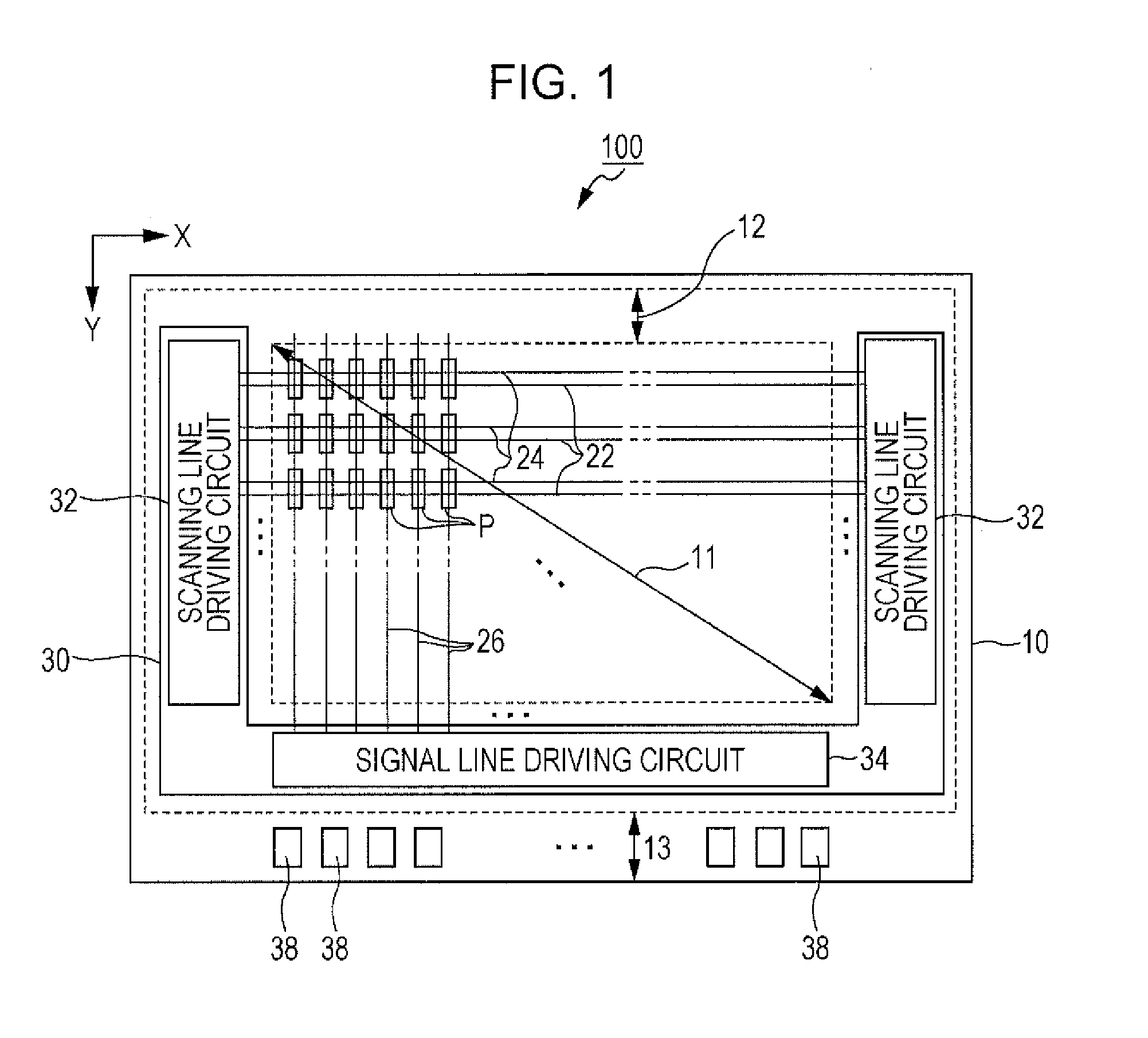
[0063]FIG. 1 is a plan view showing a light emitting apparatus 100 of the embodiment.
[0064]As shown in FIG. 1, the light emitting apparatus 100 of the embodiment is an organic EL apparatus in which the light emitting element using an organic EL material is formed on a semiconductor substrate 10. The light emitting apparatus 100 is, for example, an organic light emitting diode (OLED). The semiconductor substrate 10 is a plate-like member which is formed of a semiconductor material such as silicon and is used as a base material in which a plurality of light emitting elements are formed.
[0065]As shown in FIG. 1, a display region 11, a peripheral region 12, and a mounting region 13 are provided on the surface of the semiconductor substrate 10. The display region 11 is a region in a rectangular shape in which a plurality of pixel circuits P are arrayed. In display region 11, a plurality of scanning lines (wirings) 22 extending in an X direction, a plurality of control lines (wirings) 24 ...
second embodiment
[0189]A second embodiment differs in not providing with the compensation transistor and the reset transistor in comparison with the first embodiment.
[0190]Moreover, as to the same configuration as the embodiment described above, there are some cases where description is omitted by appropriately attaching the same reference numerals or the like.
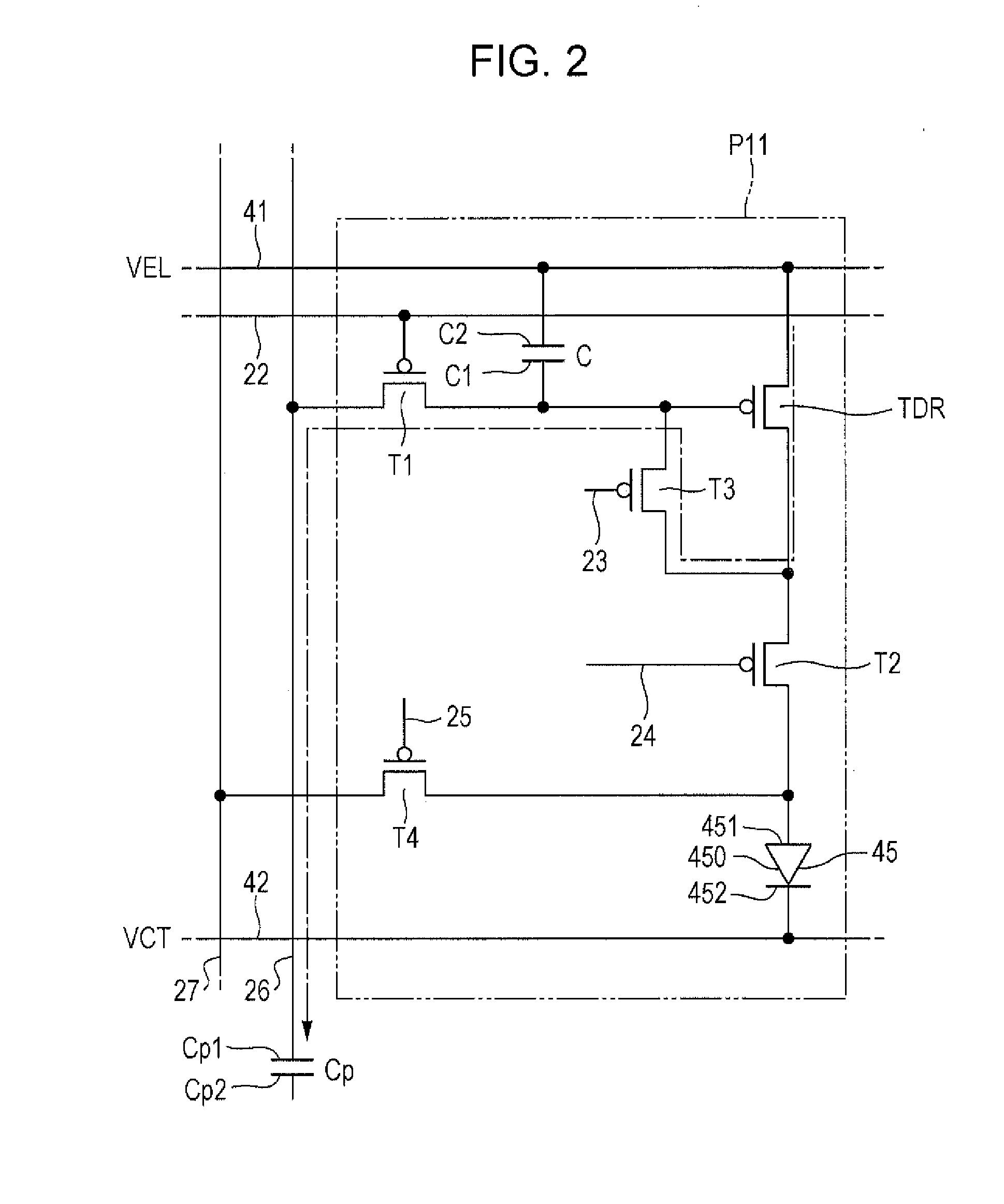
[0191]FIG. 17 is a circuit diagram showing a pixel circuit P21 of the embodiment. FIG. 18 and FIG. 19 are plan views schematically showing a pixel circuit P21 of the embodiment. In FIG. 18, an illustration of a wiring and a contact hole is omitted.
[0192]As shown in FIG. 17, the pixel circuit P21 of the embodiment is provided with a driving transistor (first transistor) TDR1, a selecting transistor T11, the light emitting control transistor T2, and the capacitive element C.
[0193]The driving transistor TDR1 and the selecting transistor T11 has the same functions as the driving transistor TDR and the selecting transistor T1 of the first embodimen...
third embodiment
[0204]The third embodiment differs in not providing with a rest transistor, with respect to the first embodiment.
[0205]Moreover, as to the same configuration as the embodiment described above, there are some cases where description will be omitted by appropriately attaching the same reference numerals.
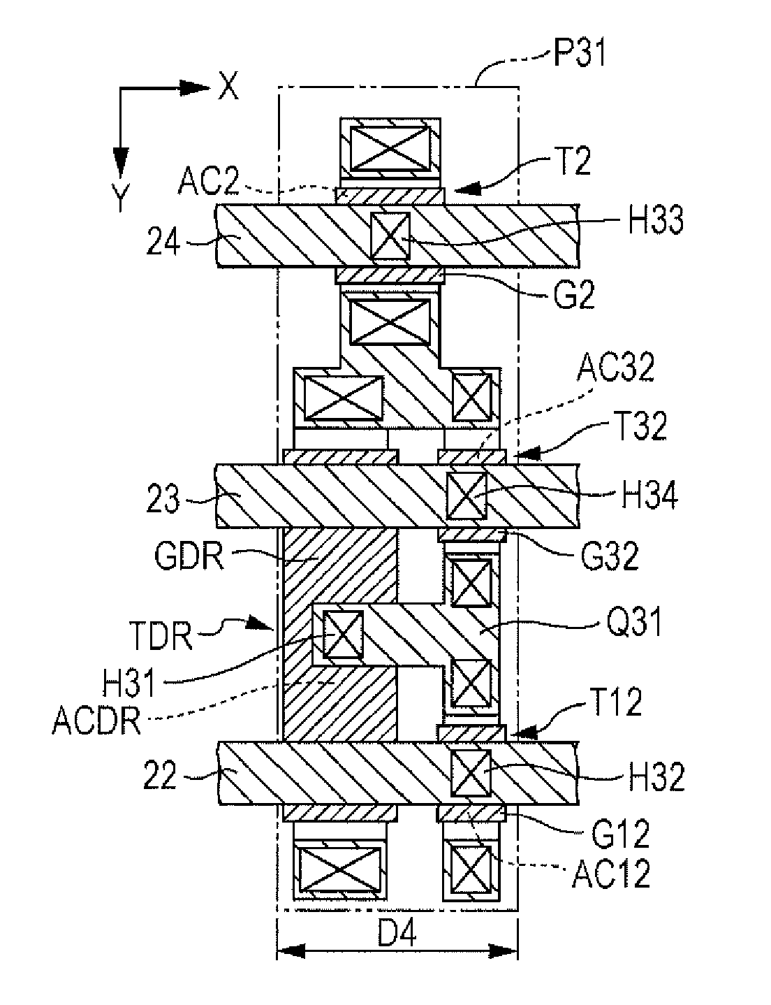
[0206]FIG. 20 is a circuit diagram showing a pixel circuit P31 of the embodiment. FIG. 21 and FIG. 22 are plan views schematically showing a pixel circuit P31 of the embodiment. In FIG. 21, an illustration of a wiring and a contact hole is omitted.
[0207]As shown in FIG. 20, the pixel circuit P31 of the embodiment is provided with the driving transistor TDR, a selecting transistor T12, the light emitting control transistor T2, a compensation transistor T32, and the capacitive element C.
[0208]The selecting transistor T12 and the compensation transistor T32 have the same functions as the selecting transistor T1 and the compensation transistor T3 of the first embodiment.
[0209]The connectio...
PUM
 Abstract
Description
Claims
Application Information