Composite sensor and composite sensor module
Active Publication Date: 2015-07-30
HAMAMATSU PHOTONICS KK
1 Cites 1 Cited by
AI-Extracted Technical Summary
Problems solved by technology
While such a sensor is required to have a sufficient detection accuracy, using a thermal image sensor such as a thermo...
Method used
[0033]Consequently, as illustrated in FIG. 1, the light-receiving parts 20 are raised from one side of the first substrate 13 while being slightly separated from the insulating film 19. As illustrated in FIG. 2, the thermal image sensors 16, 16 adjacent to each other have therebetween an arrangement pitch (distance between the centers of the light-receiving parts 20) W1 of about 60 μm, for example. A light-reflecting layer made of Al or the like may be disposed on the insulating film 19 so as to correspond to the region formed with the light-receiving parts 20. In this case, the light-reflecting layer can make leak light incident on the light-receiving parts 20, thereby further improving the sensitivity of the thermal image sensors 16.
[0047]In this composite sensor 11, as explained in the foregoing, the arrangement region R1 of the thermal image sensors 16 and the arrangement region R2 of the range image sensors 31 are arranged so as to overlap each other as seen in the mounting direction. This makes it possible to acquire thermal and range images coaxially, thereby suppressing image misalignment between the thermal and range images. Hence, an object to be detected can be detected accurately. It also reduces the time required for calculations and improves time resolution.
[0048]In this composite sensor 11, the seal body S1 formed by mounting the first and second substrates 13, 14 on top of each other seals a space about the thermal image sensors 16 in a vacuum state. This can prevent the heat occurring about the range image sensors 31 from affecting the thermal image sensor 16 side, thereby improving the sensitivity of the thermal image sensors 16. In addition, the substrate arranged with the thermal image sensors 16 and the substrate arranged with the range image sensors 31 are separate from each other, which makes it possible to perform manufacturing methods optimal for the sensors and secure a degree of freedom in designing for arranging a signal readout circuit and the like.
[0049]In the composite sensor 11, the arrangement pitch W2 of the range image sensors 31 in...
Benefits of technology
[0015]The present invention can fully improve the sensitivity of the ...
Abstract
In a composite sensor, an arrangement region of thermal image sensors and an arrangement region of range image sensors are arranged so as to overlap each other as seen in the mounting direction. This makes it possible to acquire thermal and range images coaxially, thereby suppressing image misalignment between the thermal and range images. In the composite sensor, a seal body formed by mounting the first and second substrates on top of each other seals a space about the thermal image sensors in a vacuum state. This can prevent the heat occurring about the range image sensors from affecting the thermal image sensor side. In addition, the substrate arranged with the thermal image sensors and the substrate arranged with the range image sensors are separate from each other, which can secure a degree of freedom in designing.
Application Domain
Television system detailsOptical rangefinders +9
Technology Topic
Image sensorEngineering +1
Image
Examples
- Experimental program(2)
Example
First Embodiment
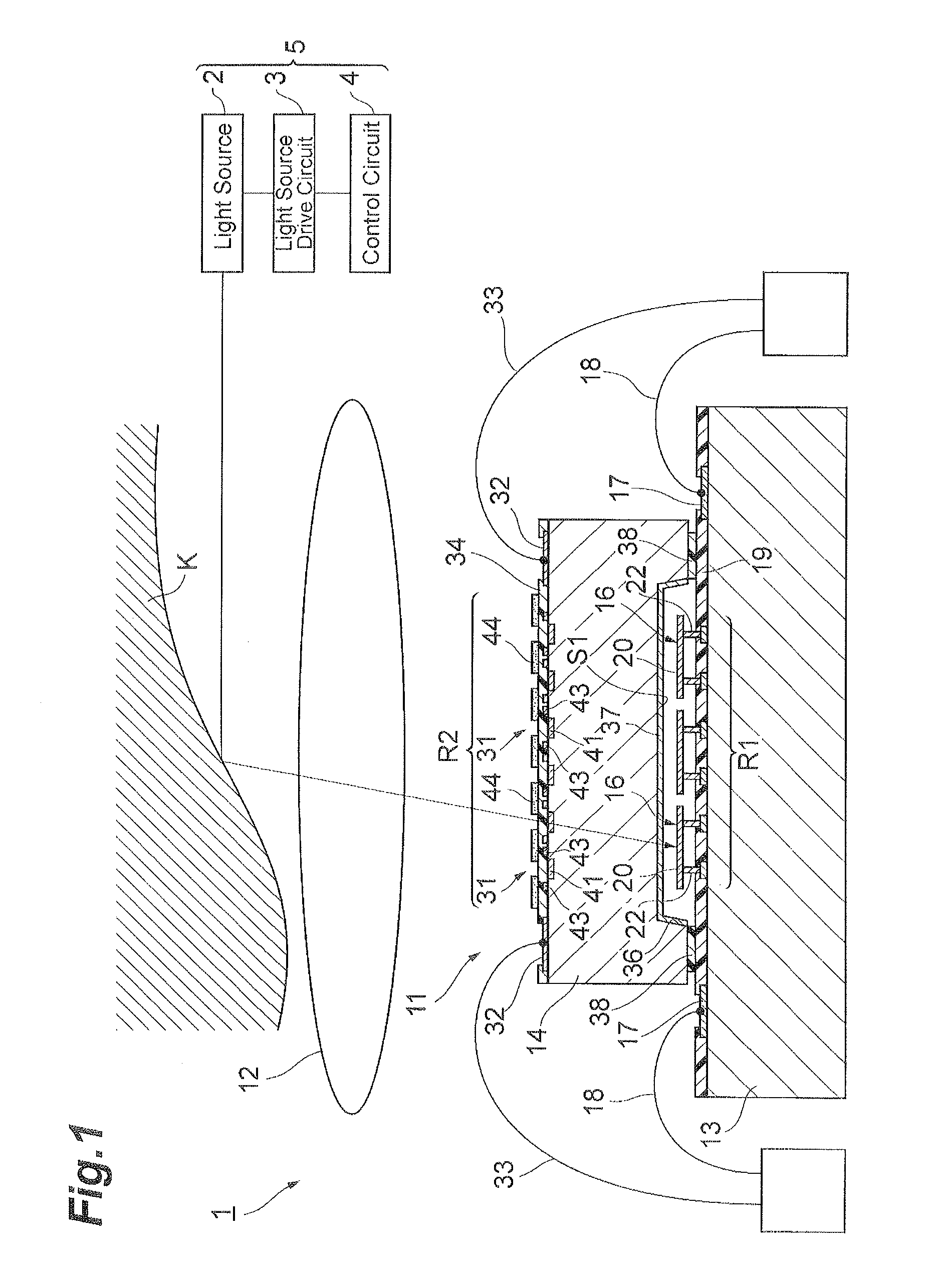
[0026]FIG. 1 is a sectional view illustrating the composite sensor module in accordance with a first embodiment of the present invention. As depicted, this composite sensor module 1 comprises a composite sensor 11 and a lens 12. The composite sensor module 1 is a module used as a motion sensor which detects entries of people into a predetermined area and the like according to thermal and range images.
[0027]Connected to the composite sensor module 1 in use is a light source unit 5 including a light source 2 such as a laser or a light-emitting diode, for example, a light source drive circuit 3 for driving the light source 2 at a high frequency, and a control circuit 4 for outputting a driving clock for the light source drive circuit 3. The light source 2 emits a modulated wave subjected to light intensity modulation in the form of a square wave or sine wave. The modulated wave is reflected by a surface of an object to be detected K and enters the composite sensor 11 through the lens 12. Preferably, the light emitted from the light source 2 is not visible light, but falls in a wavelength band where a sufficient sensitivity for Si is obtained; for example, near infrared light having a wavelength of about 800 nm is chosen. The modulated signal (charge transfer signal) in the form of the square wave or sine wave in synchronization with the driving clock from the control circuit 4 is fed to transfer electrodes 43, 43 of a range image sensor 31, which will be explained later, in respective phases on the reverse of each other.
[0028]The lens 12, which is an imaging lens made of ZnSe, for example, is arranged such as to have an imaging plane at an arrangement region R2 of range image sensors 31, which will be explained later. For example, light in a wavelength band of 0.5 μm to 28.1 μm passes through the lens 12, so as to enter the composite sensor 11. Not only ZnSe, but ZnS, As2S3, and the like may also be used as a material for the lens 12.
[0029]The composite sensor 11 will now be explained.
[0030]As illustrated in FIGS. 1 and 2, the composite sensor 11 comprises a first substrate 13 on which thermal image sensors 16 are arranged in a matrix and a second substrate 14, slightly smaller than the first substrate 13, on which range image sensors 31 are arranged in a matrix. Each of the first and second substrates 13, 14 is formed of Si by a thickness of about 30 μm, so that light in a wavelength band of 1.2 μM to 28.1 μm, for example, passes therethrough.
[0031]An arrangement region R1 of the thermal image sensors 16 is set into a substantially square form on one side of the first substrate 13. On the outside of the arrangement region R1, electrode pads 17 for the thermal image sensors 16 are arranged so as to surround the arrangement region R1. Wires 18 electrically connect the electrode pads 18 to wiring circuits on the package side. Except for the locations formed with the electrode pads 17, the one side of the first substrate 13 is covered with an insulating film 19 made of SiO2, for example.
[0032]Each of the thermal image sensors 16 arranged on the first substrate 13 is a wavelength-independent sensor such as a thermopile or bolometer, for example, and has a plurality of thermoelectric elements. As illustrated in FIG. 3, each pixel of the thermal image sensor 16 has a substantially rectangular light-receiving part 20, joints 21, 21 extending from two opposing corners of the light-receiving part 20 in respective directions opposite from each other along sides of the light-receiving part 20, and support columns 22, 22 disposed at respective leading end parts of the joints 21, 21.
[0033]Consequently, as illustrated in FIG. 1, the light-receiving parts 20 are raised from one side of the first substrate 13 while being slightly separated from the insulating film 19. As illustrated in FIG. 2, the thermal image sensors 16, 16 adjacent to each other have therebetween an arrangement pitch (distance between the centers of the light-receiving parts 20) W1 of about 60 μm, for example. A light-reflecting layer made of Al or the like may be disposed on the insulating film 19 so as to correspond to the region formed with the light-receiving parts 20. In this case, the light-reflecting layer can make leak light incident on the light-receiving parts 20, thereby further improving the sensitivity of the thermal image sensors 16.
[0034]On one side of the second substrate 14, on the other hand, the arrangement region R2 of the thermal image sensors 31 is set into a substantially square form with a size on a par with the arrangement region R1 of the thermal image sensors 16, for example, as illustrated in FIG. 1. On the outside of the arrangement region R2, the electrode pads 32 for the range image sensors 31 are arranged so as to surround the arrangement region R2 at positions on the inside of the electrode pads 32 for the thermal image sensors 31 in planar view. As with the electrode pads 17, the electrode pads 32 are electrically connected to wiring circuits on the package side with wires 33. Except for the locations formed with the electrode pads 32, the one side of the second substrate 14 is covered with an insulating film 34 made of SiO2, for example.
[0035]The other side of the second substrate 14 is formed with a depression 36 having a substantially square cross section with a size corresponding to the arrangement region R1 of the thermal image sensors 16 by anisotropic etching or dry etching of Si, for example. The inner wall surface of the depression 36 is provided with an optical filter film 37 transparent to light in a mid-infrared region. More specifically, the optical filter film 37 is constituted by a multilayer film of Ge and ZnS, for example, so as to transmit therethrough only light in a band on the order of 8 μm to 14 μm. On the other side of the second substrate 14, fringe parts of the depression 36 are provided with an insulating film 38 made of SiO2, for example.
[0036]The foregoing second substrate 14 is mounted on the first substrate 13 such that the depression 36 faces the first substrate 36, while the arrangement region R1 of the thermal image sensors 16 and the arrangement region R2 of the range image sensors 31 overlap each other as seen in the mounting direction. Mounting the second substrate 14 causes the inner wall surface of the depression 36 and one side of the first substrate 13 to form a seal body S1 which seals a space about the thermal image sensors 16 with the first substrate 13 serving as a top plate. For mounting the first and second substrates 13, 14 on top of each other, room temperature bonding in a vacuum atmosphere is used, for example. Therefore, the inner space of the seal body S1 containing the thermal image sensors 16 is in a vacuum state.
[0037]The range image sensors 31 arranged on the second substrate 14 are so-called charge distribution type range image sensors. As illustrated in FIG. 4, each pixel of the range image sensors 31 has a light-receiving part (charge generation region) 41 for generating an electric charge in response to light incident thereon and a pair of transfer electrodes 43, 43 for transferring the electric charge generated in the light-receiving part 41 to charge collection regions 42, 42 according to a charge transfer signal given beforehand.
[0038]The light-receiving parts 41, which are parts where the light transmitted through the lens 12 is incident, are arranged 2×2 for each light-receiving part 20 of the thermal image sensors 16 as illustrated in FIG. 2. As a consequence, the range image sensors 31, 31 adjacent to each other have therebetween an arrangement pitch (distance between the centers of the light-receiving parts 41) W2 which is ½ or less of the above-mentioned arrangement pitch W1 between the thermal image sensors 16, 16. In the arrangement region R2, the part excluding the light-receiving parts 41 is formed with a light-shielding part 44 made of Al, for example. The light-shielding part 44 is formed on the insulating film 34 such as to open at the portion corresponding to the light-receiving parts 41, so that the ratio of the opening portion to the light-shielding part 44 is on the order of 20% to 50%, for example.
[0039]As illustrated in FIG. 4, the charge collection regions 42, 42 are a pair of high-concentration n-type semiconductor regions further formed on the surface side of a p-type semiconductor region formed with a low concentration on the surface side of a high-concentration p-type semiconductor region. The n-type semiconductor regions have electrons as carriers in an electrically neutral state and will positively be ionized if the carriers drop out. Hence, the charge collection regions 42, 42 will greatly be depressed downward, thereby constructing a potential well. Source follower amplifiers 46, 46 are electrically connected to the charge collection regions 42, 42, respectively.
[0040]The transfer electrodes 43, 43 are arranged between the light-receiving part 41 and the charge collection regions 42, 42. The modulated signal (charge transfer signal) in the form of the square wave or sine wave in synchronization with the driving clock from the control circuit 4 is fed to the transfer electrodes 43, 43 in respective phases on the reverse of each other. A region having a potential lower than that of the light-receiving part 41 is formed directly under the transfer electrode 43 fed with the high-level modulated signal. As a consequence, the electrons generated in the light-receiving part 41 are transferred by the transfer electrode 43, so as to be distributed and stored into its corresponding charge collection region 42.
[0041]The electric charges stored in the charge collection regions 42, 42 are fed through an amplification circuit and the like to the control circuit 4 as outputs from the source follower amplifiers 46, 46. According to the outputs from the source follower amplifiers 46, 46, the control circuit 4 calculates a distance, for example, by L=(½)×c×[Q2/(Q1+Q1)]×T0, where c is the velocity of light, Q1 is the output signal on the transfer electrode VTX1 side (output signal with a phase of 0°), Q2 is the output signal on the transfer electrode VTX2 side (output signal with a phase of 180°), and T0 is the pulse width.
[0042]Steps of manufacturing the composite sensor 11 will now be explained.
[0043]For manufacturing the composite sensor 11, the first and second substrates 13, 14 are prepared separately from each other as illustrated in FIG. 5(a). The electrode pads 17 and insulating film 19 are formed beforehand as a pattern on the first substrate 13, and the thermal image sensors 16 are arranged in the arrangement region R1. The second substrate 14 is formed with the depression 36 by anisotropic etching or dry etching of Si, and then the optical filter film 37 is formed on the inner wall surface of the depression 36 by vapor deposition and the like. Thereafter, individual constituents of the electrode pads 32, insulating films 34, 38, light-shielding part 44, and range image sensors 31 are formed as a pattern.
[0044]Subsequently, as illustrated in FIG. 5(b), the second substrate 14 is mounted on the first substrate 13 by room temperature bonding such that the depression 36 faces the first substrate 13, while the arrangement region R1 of the thermal image sensors 16 and the arrangement region R2 of the range image sensors 31 overlap each other as seen in the mounting direction. This forms the seal body S1 sealing a space about the thermal image sensors 16 with the first substrate 13 serving as a top plate. Joining the second substrate 14 to the first substrate 13 at room temperature in a vacuum atmosphere can make the seal body S1 have a vacuum state therewithin.
[0045]After mounting the second substrate 14 on the first substrate 13, the first and second substrates 13, 14 are irradiated with laser light along predetermined lines to cut as illustrated in FIG. 6(a), so as to form modified layers 48 therewithin. From the viewpoint of workability, it is preferred for the first substrate 13 to be formed with the modified layers 48 before the second substrate 14.
[0046]After forming the modified layers 48, an expandable sheet 49 is attached to the other side of the second substrate 14, for example. Then, the expandable sheet 49 is expanded in its in-plane directions, so as to cut the first and second substrates 13, 14 along the modified layers 48 as illustrated in FIG. 6(b). This separates the individual devices of the composite sensors 11 from each other, thereby yielding the composite sensor 11 illustrated in FIG. 1.
[0047]In this composite sensor 11, as explained in the foregoing, the arrangement region R1 of the thermal image sensors 16 and the arrangement region R2 of the range image sensors 31 are arranged so as to overlap each other as seen in the mounting direction. This makes it possible to acquire thermal and range images coaxially, thereby suppressing image misalignment between the thermal and range images. Hence, an object to be detected can be detected accurately. It also reduces the time required for calculations and improves time resolution.
[0048]In this composite sensor 11, the seal body S1 formed by mounting the first and second substrates 13, 14 on top of each other seals a space about the thermal image sensors 16 in a vacuum state. This can prevent the heat occurring about the range image sensors 31 from affecting the thermal image sensor 16 side, thereby improving the sensitivity of the thermal image sensors 16. In addition, the substrate arranged with the thermal image sensors 16 and the substrate arranged with the range image sensors 31 are separate from each other, which makes it possible to perform manufacturing methods optimal for the sensors and secure a degree of freedom in designing for arranging a signal readout circuit and the like.
[0049]In the composite sensor 11, the arrangement pitch W2 of the range image sensors 31 in the second substrate 14 is smaller than the arrangement pitch W1 of the thermal image sensors 16 in the first substrate 13. The range image sensors 31 include constituents such as the transfer electrodes 43, and these constituents may become a shield which covers the thermal image sensors 16. Therefore, when the arrangement pitch W2 of the range image sensors 31 is on a par with or greater than the arrangement pitch W1 of the thermal image sensors 16, the influence of shield per pixel of the thermal image sensors 16 may be so large that thermal images deteriorate their quality. Hence, making the arrangement pitch W2 of the range image sensors 31 smaller than the arrangement pitch W1 of the thermal image sensors 16 can suppress the influence of shield per pixel of the thermal image sensors 16, thereby securing the thermal image quality.
[0050]In the composite sensor 11, the optical filter film 37 transparent to light in a mid-infrared region is formed on an inner wall surface of the seal body S1. This can cut off light in a wavelength band which is susceptible to the absorption by moisture, carbon dioxide, and the like in air, thereby enabling the thermal image sensors 16 to further improve their sensitivity.
Example
Second Embodiment
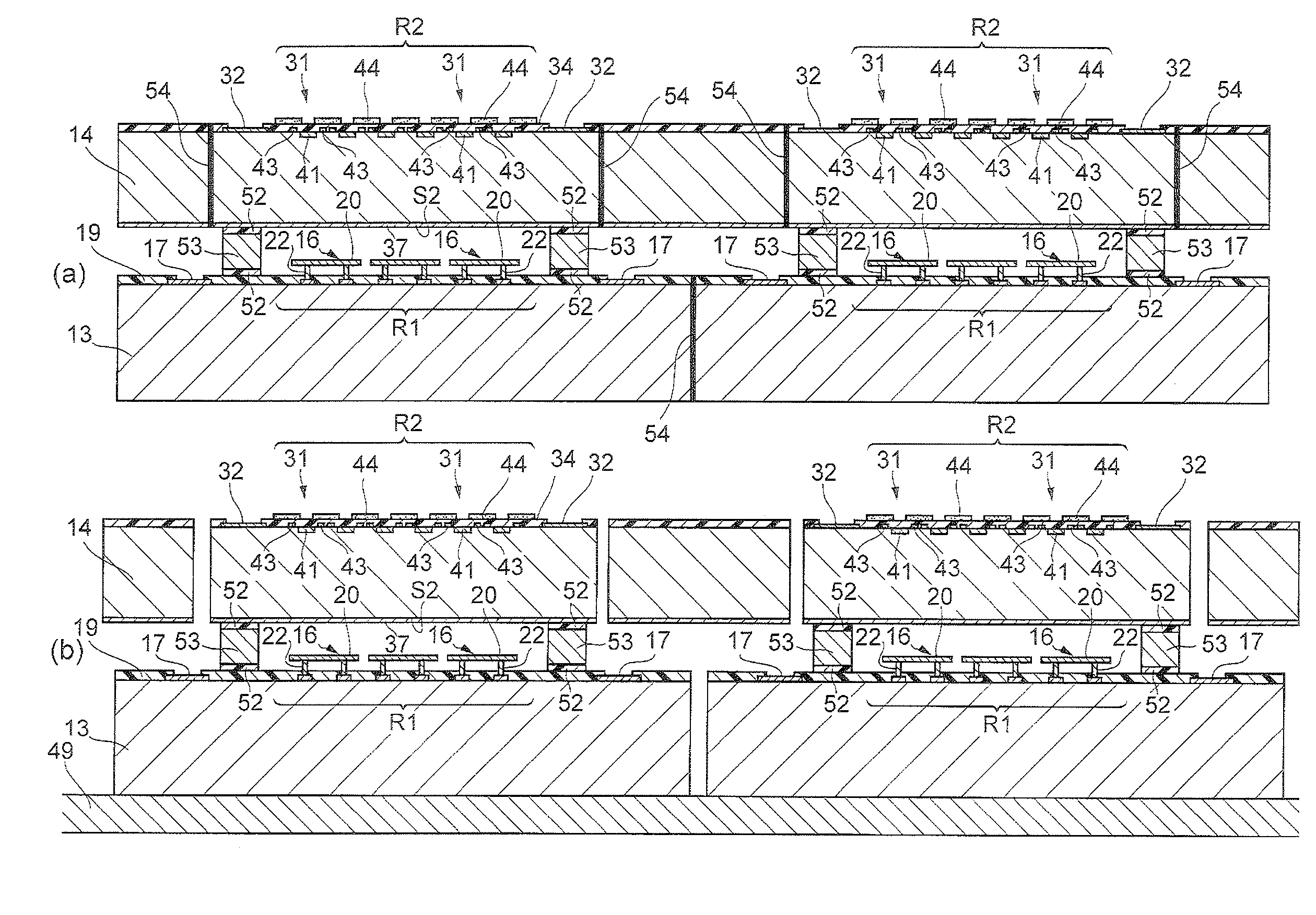
[0051]FIG. 7 is a sectional view illustrating a composite sensor module 50 in accordance with a second embodiment of the present invention. As depicted, the composite sensor module 50 in accordance with the second embodiment differs from the first embodiment in the joint structure between the first and second substrates 13, 14 in the composite sensor 51.
[0052]More specifically, the composite sensor 51 has no depression 36 on the other side of the second substrate 14, so that the second substrate 14 has a flat surface on the other side. The optical filter film 37 is formed all over the surface on the other side of the second substrate 14. For joining the first and second substrates 13, 14 together, foil materials 52 and a lid material 53 are used. The foil materials 52, each of which is a layer combining a buffer metal with a low-melting metal, are made of Ti/Pt/Au or Cr/Ni/Au, for example. The foil materials 52 are arranged like rings on one side of the first substrate 13 and the other side of the second substrate 14 at positions overlapping the electrode pads 32, for example.
[0053]The lid material 53 is a ring-shaped metal material made of Kovar, for example. The lid material 53 is held between and joined to the foil material 52 on the first substrate 13 side and the foil material 52 on the second substrate side. Since the lid material 53 is interposed, a space corresponding to the thickness of the lid material 53 is formed between the first and second substrates 13, 14. One side of the first substrate 13, the other side of the second substrate 14, and the lid material 53 form a seal body S2 sealing a space about the thermal image sensors 16 with the first substrate 13 serving as a top plate. The inner space of the seal body S2 has a vacuum state as in the first embodiment.
[0054]For manufacturing the composite sensor 51, the first and second substrates 13, 14 are prepared separately from each other as illustrated in FIG. 8(a). The electrode pads 17, insulating film 19, and foil material 52 are formed beforehand as a pattern on the first substrate 13, and the thermal image sensors 16 are arranged in the arrangement region R1. The second substrate 14 is formed beforehand with individual constituents of the electrode pads 32, insulating films 34, 38, foil material 52, light-shielding part 44, and range image sensors 31 as a pattern after forming the optical filter film 37 on the other side by vapor deposition, for example.
[0055]Subsequently, as illustrated in FIG. 8(b), the lid material 53 is arranged between the foil materials 52, 52 while the arrangement region R1 of the thermal image sensors 16 and the arrangement region R2 of the range image sensors 31 overlap each other as seen in the mounting direction, and the second substrate 14 is mounted on the first substrate 13. This forms the seal body S2 sealing a space about the thermal image sensors 16 with the first substrate 13 serving as a top plate. Joining them in a vacuum atmosphere can place the inner space of the seal body S2 into a vacuum state.
[0056]After mounting the second substrate 14 on the first substrate 13, the first and second substrates 13, 14 are irradiated with laser light along predetermined lines to cut as illustrated in FIG. 9(a), so as to form modified layers 54 therewithin. From the viewpoint of workability, it is preferred for the first substrate 13 to be formed with the modified layers 54 before the second substrate 14.
[0057]After forming the modified layers 54, an expandable sheet 49 is attached to the other side of the second substrate 14, for example.
[0058]Then, the expandable sheet 49 is expanded in its in-plane directions, so as to cut the first and second substrates 13, 14 along the modified layers 54 as illustrated in FIG. 9(b). This separates the individual devices of the composite sensor 51 from each other, thereby yielding the composite sensor 51 illustrated in FIG. 7.
[0059]In the foregoing composite sensor 51, the arrangement region R1 of the thermal image sensors 16 and the arrangement region R2 of the range image sensors 31 are also arranged so as to overlap each other as seen in the mounting direction. This makes it possible to acquire thermal and range images coaxially, thereby suppressing image misalignment between the thermal and range images. Hence, an object to be detected can be detected accurately. It also reduces the time required for calculations and improves time resolution.
[0060]In this composite sensor 51, the seal body S2 formed by mounting the first and second substrates 13, 14 on top of each other also seals a space about the thermal image sensors 16 in a vacuum state. This can prevent the heat occurring about the range image sensors 31 from affecting the thermal image sensor 16 side, thereby improving the sensitivity of the thermal image sensors 16. In addition, the substrate arranged with the thermal image sensors 16 and the substrate arranged with the range image sensors 31 are separate from each other, which makes it possible to perform manufacturing methods optimal for the sensors and secure a degree of freedom in designing for arranging a signal readout circuit and the like.
[0061]In this composite sensor 51, the arrangement pitch W2 of the range image sensors 31 in the second substrate 14 is also smaller than the arrangement pitch W1 of the thermal image sensors 16 in the first substrate 13, This can suppress the influence of shield per pixel of the thermal image sensors 16, thereby securing the thermal image quality, Further, the optical filter film 37 within the seal body S2 can cut off light in a wavelength band which is susceptible to the absorption by moisture, carbon dioxide, and the like in air, thereby enabling the thermal image sensors 16 to further improve their sensitivity.
REFERENCE SIGNS LIST
[0062]1, 50: composite sensor module; 11, 51: composite sensor; 12: lens; 13: first substrate; 14: second substrate; 16: thermal image sensor; 31: range image sensor; 37: optical filter film; 41: light-receiving part (charge generation region); 42: charge collection region; 43: transfer electrode; R1: arrangement region of thermal image sensors; R2: arrangement region of range image sensors; S1, S2: seal body; W1: arrangement pitch of thermal image sensors; W2: arrangement pitch of range image sensors.
PUM


Description & Claims & Application Information
We can also present the details of the Description, Claims and Application information to help users get a comprehensive understanding of the technical details of the patent, such as background art, summary of invention, brief description of drawings, description of embodiments, and other original content. On the other hand, users can also determine the specific scope of protection of the technology through the list of claims; as well as understand the changes in the life cycle of the technology with the presentation of the patent timeline. Login to view more.
Similar technology patents
Gated range scanning lfmcw radar structure
Owner:INTELLIGENT FUSION TECH
Silicon condenser microphone having an additional back chamber and a fabrication method therefor
Owner:BSE CO LTD
Multispectral optical sensor and method of manufacturing the same
Owner:KOREA ELECTRONICS TECH INST
Image sensor and method for manufacturing the same
Owner:MARVELL ASIA PTE LTD
Gas sensor with sensing particle receptacles
Owner:HON HAI PRECISION IND CO LTD
Classification and recommendation of technical efficacy words
- improve sensitivity
- secure degree of freedom
Gamma ray detector for positron emission tomography (pet) and single photon emisson computed tomography (spect)
Owner:EUROPEAN ORGANIZATION FOR NUCLEAR RESEARCH
Ir emitter and ndir sensor
Owner:SCIOSENSE BV
Dual loop sensing scheme for resistive memory elements
Owner:OVONYX MEMORY TECH LLC
Miniaturized lateral flow device for rapid and sensitive detection of proteins or nucleic acids
Owner:LOS ALAMOS NATIONAL SECURITY
Exhaust device
InactiveUS20050082113A1enhance appearance qualitysecure degree of freedom
Owner:HONDA MOTOR CO LTD