
Scribe line structure

Active Publication Date: 2015-07-30
UNITED MICROELECTRONICS CORP
View PDF12 Cites 8 Cited by
  • Summary
  • Abstract
  • Description
  • Claims
  • Application Information

AI Technical Summary

Benefits of technology

The present invention provides a new structure called a scribe line that helps prevent damage to electronic components during the process of dicing. The structure includes a patterned metal layer made of many small patterns right below a pad, which helps to reduce the risk of chipping and cracking. This layer is divided into many smaller patterns, which makes it easier to remove any debris during the cutting process. Overall, this new structure helps to improve the reliability and efficiency of electronic components.

Problems solved by technology

However, for achieving low dielectric property, many of low dielectric materials have loose and weak mechanical strength structures, and are fragile.
Therefore a chip crack often occurs from lateral cutting stress while performing wafer dicing.
The chip crack damages the die seal ring region of the wafer that protects the die region and induces metal layer delamination.
This causes high early failure rate in products, thereby reducing yield in subsequent electric test processes.

Method used


Image

  • Scribe line structure
  • Scribe line structure
  • Scribe line structure

Examples


Embodiment Construction

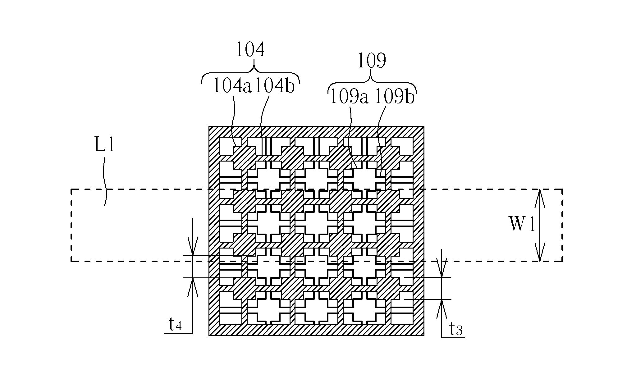
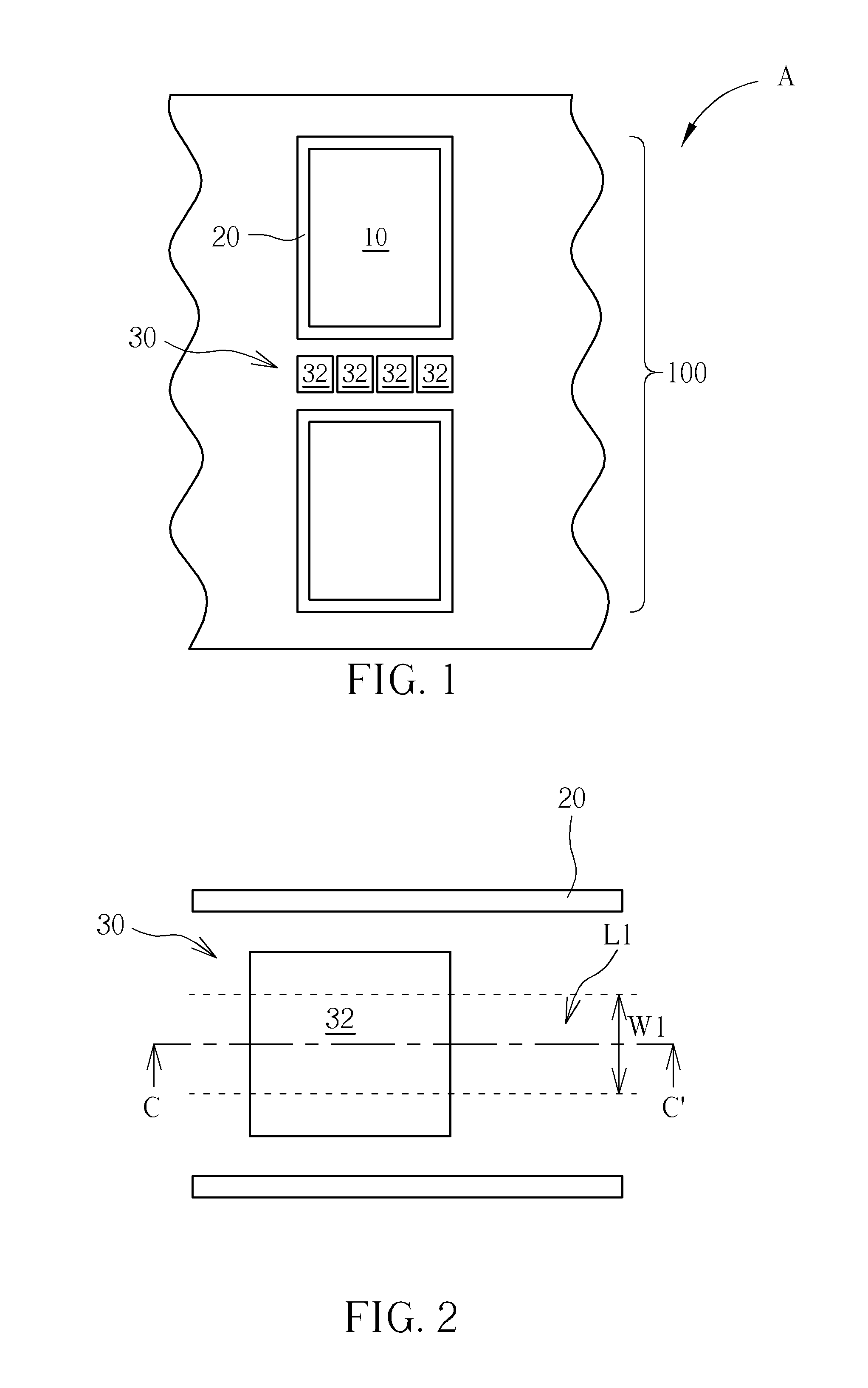
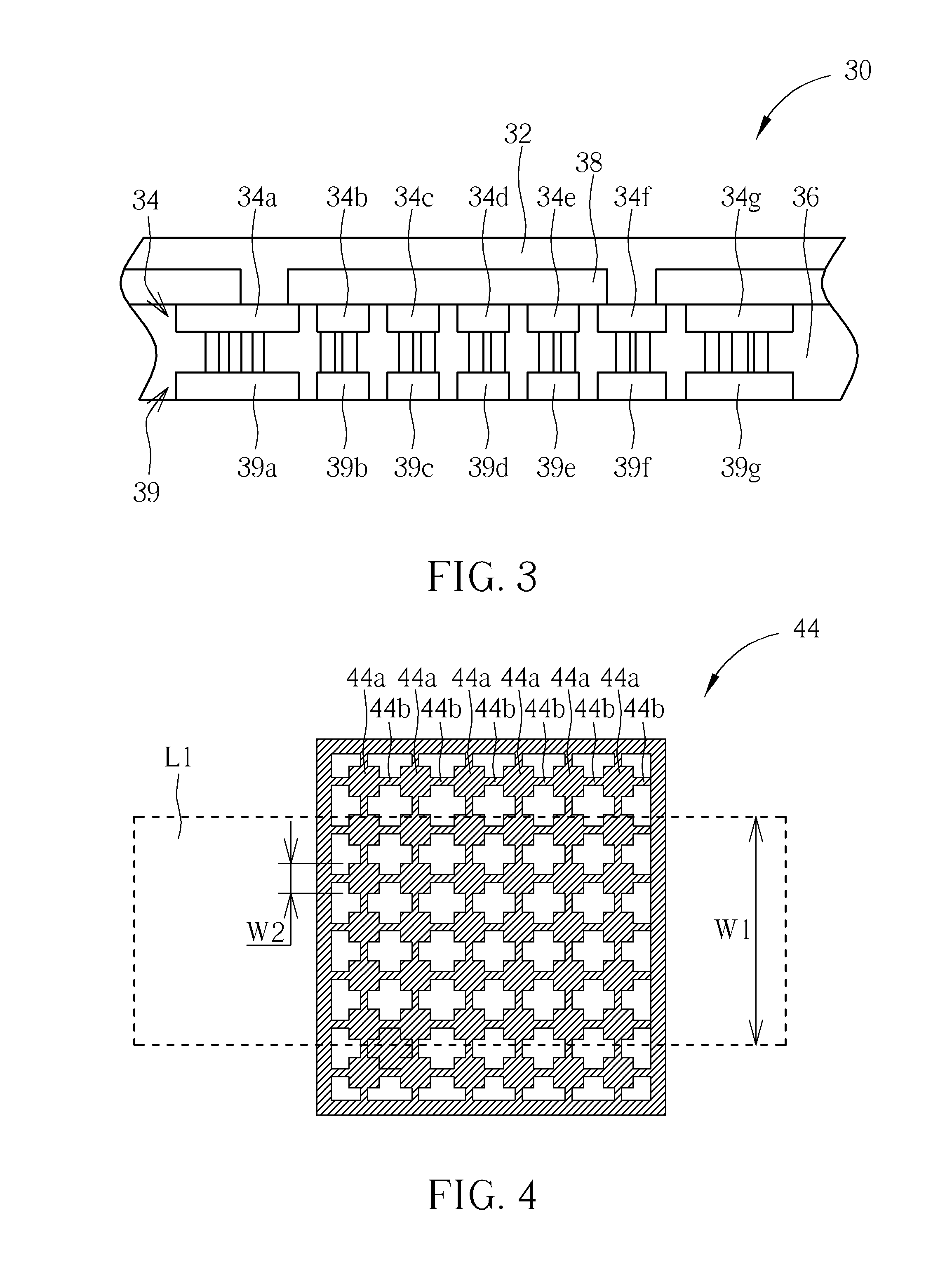
[0020]FIG. 1 schematically depicts a top view of a scribe line structure according to an embodiment of the present invention. As shown in FIG. 1, a scribe line structure A includes a semiconductor substrate 100. The semiconductor substrate 100 may be a silicon substrate, a silicon containing substrate, a III-V group-on-silicon (such as GaN-on-silicon) substrate, a graphene-on-silicon substrate or a silicon-on-insulator (SOI) substrate or others. The semiconductor substrate 100 may can be divided into a die region 10, a die sealing region 20 and a dicing region 30 (or called a scribe line) according to their purposes. The die sealing region 20 is located outside the die region 10. The dicing region 30 is located outside the die sealing region 20. Thus, the die sealing region 20 is disposed between the die region 10 and the dicing region 30, so that the die sealing region 20 can serve as a blocking wall for preventing the die region 10 from external stress while the semiconductor subs...


PUM


Abstract

A scribe line structure including a semiconductor substrate, a pad and a first patterned metal layer is provided. The semiconductor substrate has a die region, a die sealing region located outside the die region and a dicing region located outside the die sealing region. The pad is disposed in the dicing region. The first patterned metal layer is disposed in the dicing region, right below and connected to the pad, wherein the first patterned metal layer has a plurality of first patterns directly connected to each other.

Description

BACKGROUND OF THE INVENTION[0001]1. Field of the Invention[0002]The present invention relates generally to a scribe line structure, and more specifically to a scribe line structure capable of preventing dicing cracks.[0003]2. Description of the Prior Art[0004]The manufacturing flow of the integrated circuit can be mainly distinguished into three stages as follows: (1) the manufacturing of the substrate, (2) the fabrication of the integrated circuit on the substrate, and (3) the cutting, electric testing, sorting, and packaging of the integrated circuit. When fabricating the integrated circuit on the substrate, the whole substrate is divided uniformly into mail repetitive dies, and the adjacent dies are separated by scribe lines. The cutting step of the integrated circuit utilizes a cutter to cut the substrate into individual dies along the scribe lines.[0005]In recent years, the high integration semiconductor process with an inter-metal dielectric layer collocated by the dual damasc...

Claims


Application Information

Patent Timeline
IPC IPC(8): H01L21/66
CPCH01L22/32H01L22/34
Inventor TANG, KUANG-HUI
Owner UNITED MICROELECTRONICS CORP
Learn More