Wiring structure and electronic device employing the same

Inactive Publication Date: 2015-08-20
SAMSUNG ELECTRONICS CO LTD
View PDF20 Cites 17 Cited by
  • Summary
  • Abstract
  • Description
  • Claims
  • Application Information

AI Technical Summary

Benefits of technology

[0008]Example embodiments relate to a wiring structure capable of reducing a line width and a wir

Problems solved by technology

A current interconnect technology has approached a physical limit in that a spec

Method used


Image

  • Wiring structure and electronic device employing the same
  • Wiring structure and electronic device employing the same
  • Wiring structure and electronic device employing the same

Examples


Embodiment Construction

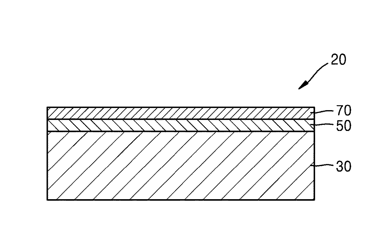
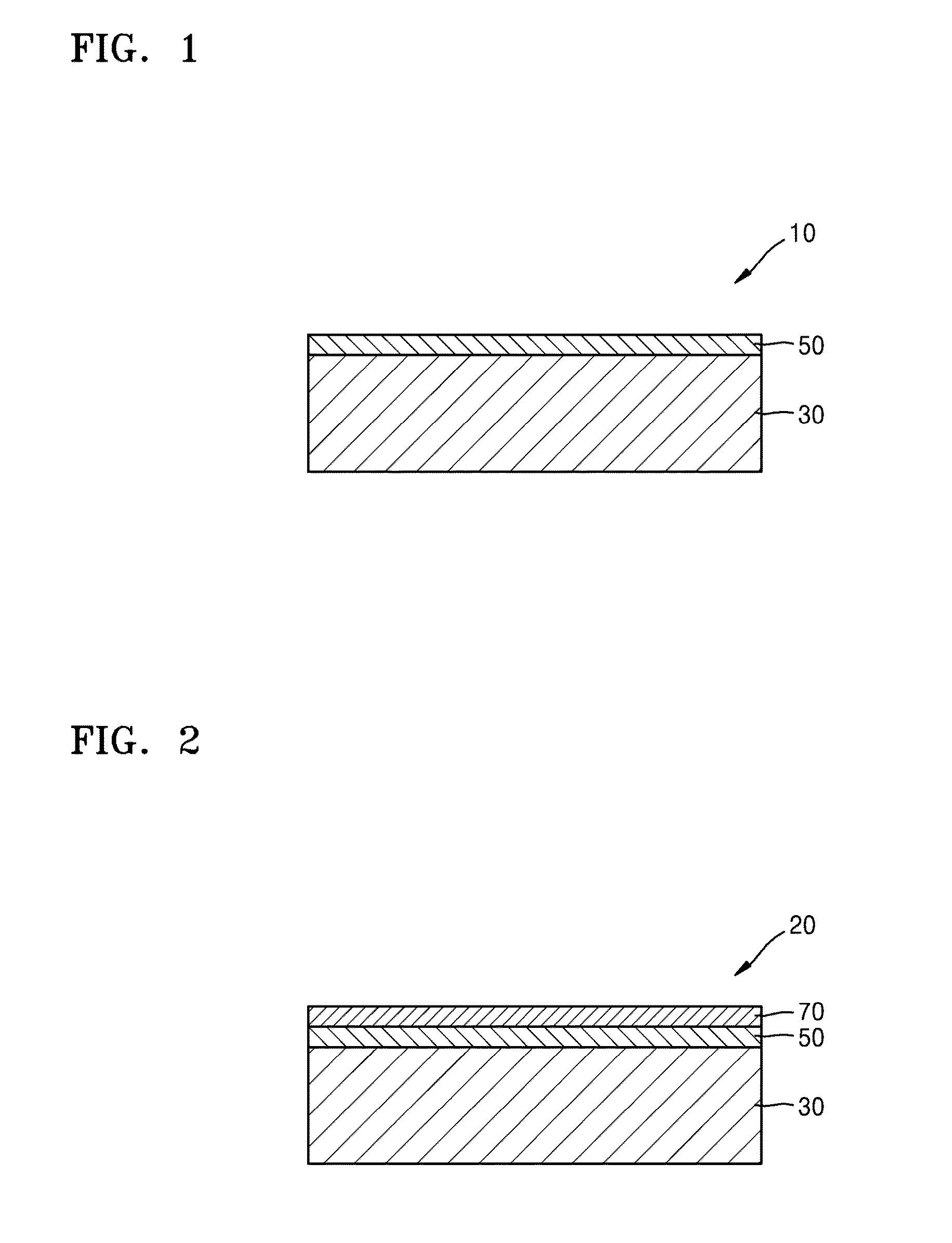
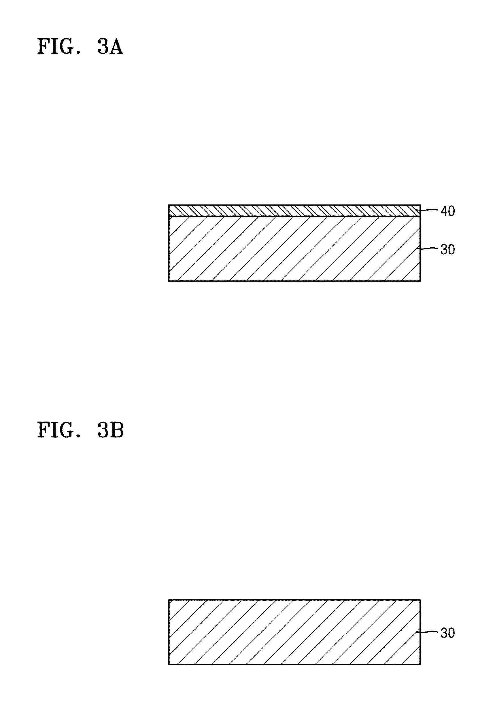
[0058]It will be understood that when an element is referred to as being “on,”“connected” or “coupled” to another element, it can be directly on, connected or coupled to the other element or intervening elements may be present. In contrast, when an element is referred to as being “directly on,”“directly connected” or “directly coupled” to another element, there are no intervening elements present. As used herein the term “and / or” includes any and all combinations of one or more of the associated listed items. Further, it will be understood that when a layer is referred to as being “under” another layer, it can be directly under or one or more intervening layers may also be present. In addition, it will also be understood that when a layer is referred to as being “between” two layers, it can be the only layer between the two layers, or one or more intervening layers may also be present.

[0059]It will be understood that, although the terms “first”, “second”, etc. may be used herein to ...


PUM


Abstract

Example embodiments relate to a wiring structure, a method of forming the same, and an electronic device employing the same. The wiring structure includes a first conductive material layer and a nanocrystalline graphene layer on the first conductive material layer in direct contact with the metal layer.

Description

RELATED APPLICATIONS[0001]This application claims priority from Korean Patent Application Nos. 10-2014-0019211, filed on Feb. 19, 2014, and 2014-149331, filed on Oct. 30, 2014, in the Korean Intellectual Property Office, the disclosure of each of which being incorporated herein in its entirety by reference.BACKGROUND[0002]1. Field[0003]Example embodiments relate to a wiring structure and / or an electronic device employing the same, more particularly, example embodiments relate to a wiring structure capable of reducing a line width and decreasing a wiring resistance, and / or an electronic device employing the same.[0004]2. Description of the Related Art[0005]Regarding high-density and high-performance semiconductor devices, efforts to reduce a line width and a thickness of a metal wiring have been made. When the line width and the thickness of the metal wiring are reduced, the number of semiconductor chips to be accumulated for each wafer may be increased. In addition, when the thickne...

Claims


Application Information

Patent Timeline
IPC IPC(8): H01L23/532H01L27/108
CPCH01L23/53276H01L23/53228H01L27/10897H01L23/53238H01L23/53252H01L23/53266H01L2924/0002H01L2924/00
Inventor LEE, CHANGSEOKSHIN, HYEONJINPARK, SEONGJUNIM, DONGHYUNPARK, HYUNSHIN, KEUNWOOKLEE, JONGMYEONGLIM, HANJIN
Owner SAMSUNG ELECTRONICS CO LTD
Why Eureka
Try Eureka