Transistor, semiconductor device and method of manufacturing the same
- Summary
- Abstract
- Description
- Claims
- Application Information
AI Technical Summary
Benefits of technology
Problems solved by technology
Method used
Image

Examples
Embodiment Construction
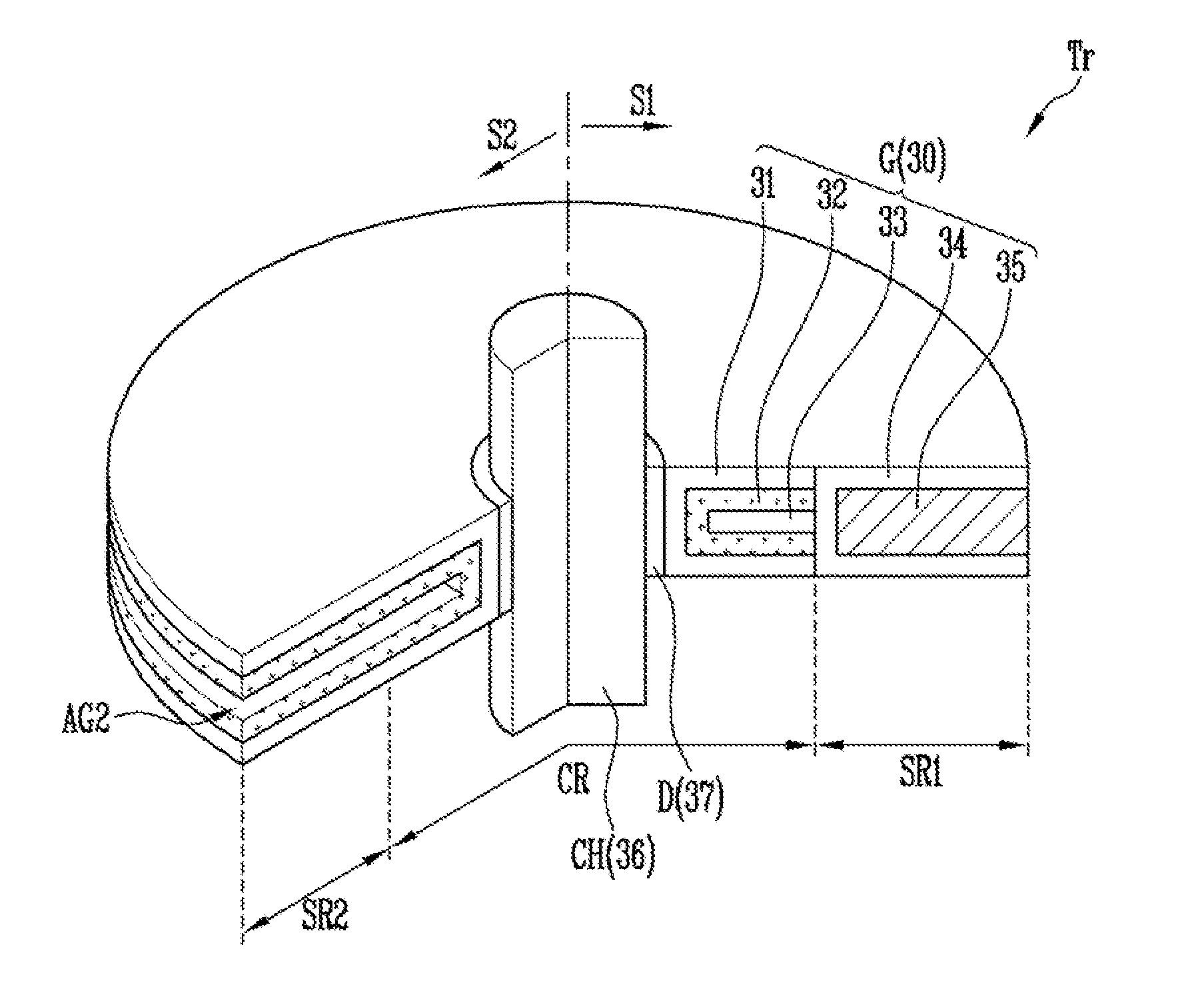
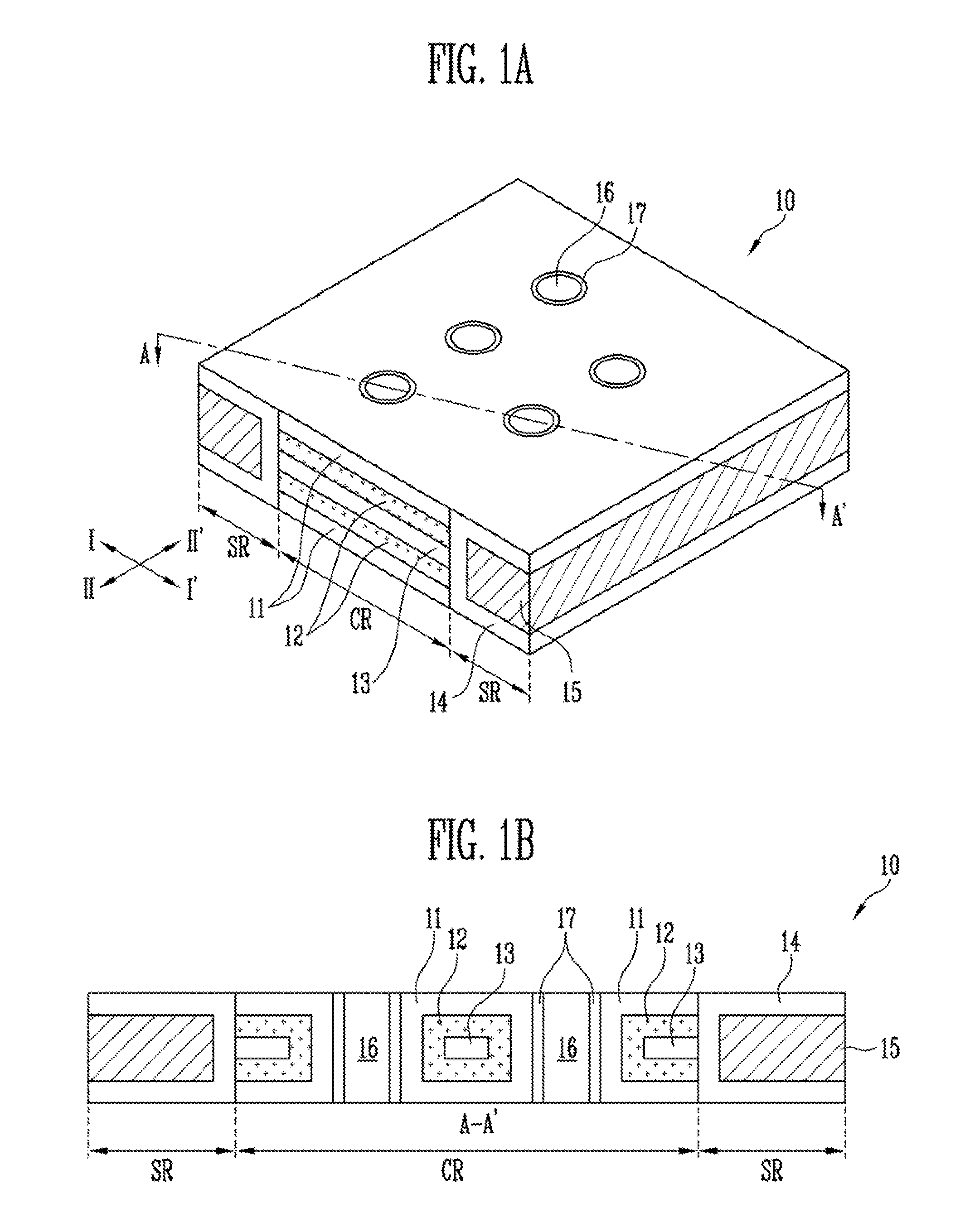
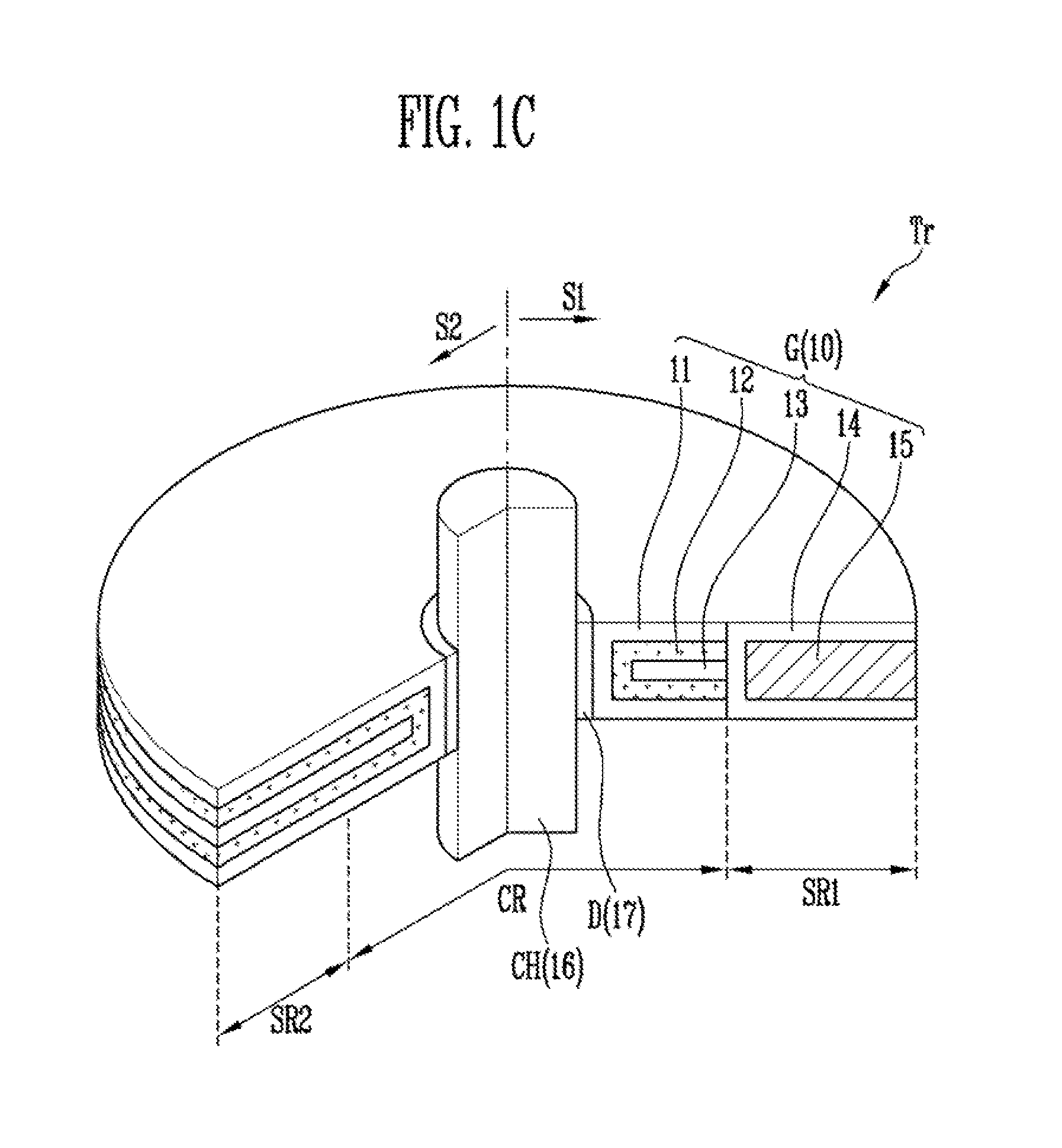
[0024]Hereinafter, preferred embodiments of the present invention will be described. In the drawings, elements and regions are not drawn to scale, and their sizes and thicknesses may be exaggerated for clarity. In the description of the present invention, known configurations that are not central to the principles of the present invention may be omitted. Throughout the drawings and corresponding description, the same components are denoted by the same reference numerals.
[0025]In presenting a specific example in a drawing or description having two or more layers in a multi-layer structure, the relative positioning relationship of such layers or the sequence of arranging the layers as shown reflects a particular implementation for the described or illustrated example and a different relative positioning relationship or sequence of arranging the layers may be possible. In addition, a described or illustrated example of a multi-layer structure may not reflect all layers present in that ...
PUM
 Abstract
Description
Claims
Application Information