

Method of processing target object and plasma processing apparatus
- Summary
- Abstract
- Description
- Claims
- Application Information
AI Technical Summary
Benefits of technology
Problems solved by technology
Method used
Image

Examples
experimental examples 1 and 2
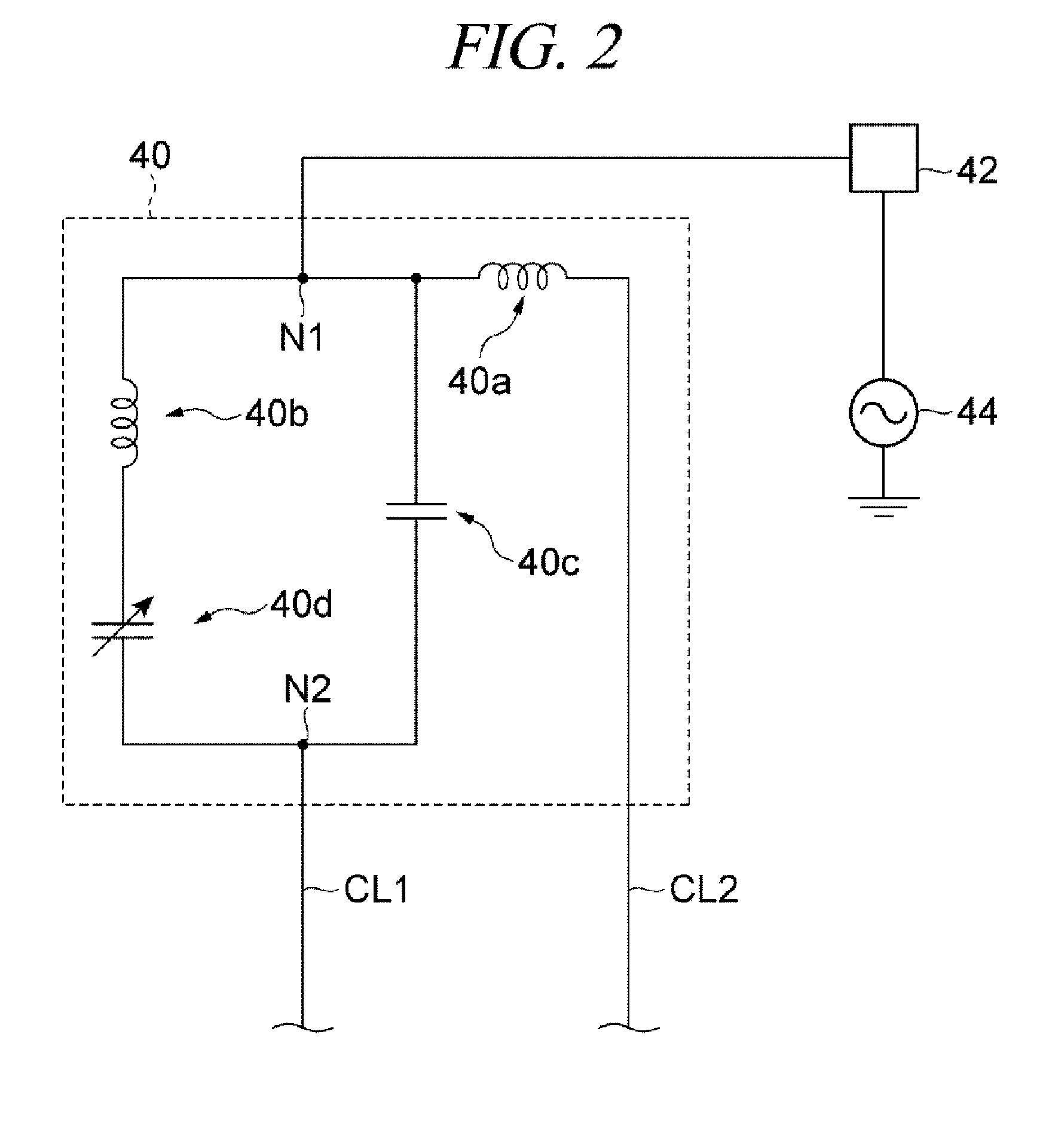
[0102]A curing process (process S1) is performed on a resist mask PRM of a target object W having a diameter of 300 mm in Experimental Examples 1 and 2 where a distance between the mounting table 14 and the upper electrode 34 is set to 35 mm and 130 mm, respectively. In each of the Experimental Examples 1 and 2, a resist mask which has a thickness of 75 nm and a line-and-space pattern with a line of a width of 50 nm and a space of a width of 50 nm is used as the resist mask PRM. Further, in both of the Experimental Examples 1 and 2, a processing time of the process S1 is varied as a parameter. The other conditions for the Experimental Examples 1 and 2 are as follows. In the following, the step number of the variable capacitor 40d, i.e., CPI is a unit of changing a capacitance of the variable capacitor 40d, and a value of CPI is proportional to the capacitance of the variable capacitor 40d.
[0103]Pressure within the processing vessel 12: 50 mTorr (6.66 Pa)
[0104]Frequency of a high fr...
experimental examples 3 to 6
[0118]In Experimental Example 3, a target object having a resist mask evenly formed on a substrate having a diameter of 300 mm is prepared, and the resist mask is etched by using a mixture gas of a CF4 gas and an O2 gas, while varying a flow rate of the O2 gas as a parameter. In Experimental Example 4, a target object having a SiO2 layer evenly formed on a substrate having a diameter of 300 mm is prepared, and the SiO2 layer is etched by using a mixture gas of a CF4 gas and an O2 gas, while varying a flow rate of the O2 gas as a parameter. In the etching by the mixture gas of the CF4 gas and the O2 gas as the etchant gas, SiO2 has a similar characteristic to that of a material forming a hard mask layer. Below are the other conditions for the Experimental Examples 3 and 4.
[0119]Pressure within the processing vessel 12: 50 mTorr (6.66 Pa)
[0120]Frequency of a high frequency power of the high frequency power supply 44: 60 MHz
[0121]Power of the high frequency power of the high frequency ...
experimental examples 7 to 9
[0149]A hard mask layer of a target object having a diameter of 300 mm is etched in Experimental Examples 7 to 9 where a distance between the mounting table 14 and the upper electrode 34 is set to 87 mm, 130 mm and 170 m, respectively. In each of the Experimental Examples 7 to 9, the target object includes, as a hard mask layer HL, a SOH layer HL2 with a thickness of 100 nm formed on the target object; and an antireflection film (Si-ARC) HL4 formed on the SOH layer HL2. Further, the target object also includes, as a resist mask PRM, an ArF resist mask with a thickness of 120 nm formed on the Si-ARC. The resist mask has a line-and-space pattern having a line with a width of 50 nm and a space with a width of 50 nm. Below are the other conditions for the Experimental Examples 7 to 9.
[0150]
[0151]Pressure within the processing vessel 12: 10 mTorr (1.33 Pa)
[0152]Frequency of a high frequency power of the high frequency power supply 44: 60 MHz
[0153]Power of the high frequency power of the ...
PUM
| Property | Measurement | Unit |
|---|---|---|
| Electric potential / voltage | aaaaa | aaaaa |
| Distance | aaaaa | aaaaa |
| Frequency | aaaaa | aaaaa |
Abstract
Description
Claims
Application Information