Semiconductor structure and forming method thereof

Active Publication Date: 2021-12-16
SEMICON MFG INT (SHANGHAI) CORP +1
View PDF0 Cites 2 Cited by
  • Summary
  • Abstract
  • Description
  • Claims
  • Application Information

AI Technical Summary

Benefits of technology

[0010]In embodiments and implementations of the present disclosure, a mandrel layer is formed on a base to occupy a position of a second trench. Compared with a solution of directly forming a second trench in a pattern transfer layer, the mandrel layer protrudes from the base. Therefore, it is easy to form the mandrel layer with a relatively small size, and the size and position of the mandrel layer have relatively high accuracy, which is correspondingly beneficial to accurately controlling pattern accuracy of the subsequently formed second trench. Moreover, after the spacer layer covering the side wall of the mandrel layer is formed, the pattern transfer layer is form

Problems solved by technology

In the development process of the ICs, generally, as a functional density (that is, a quantity of interconnection structures per chip) gradually increases, the geometric size (that is, the smallest component size that can be produced by using process steps) gradually

Method used


Image

  • Semiconductor structure and forming method thereof
  • Semiconductor structure and forming method thereof
  • Semiconductor structure and forming method thereof

Examples


Example

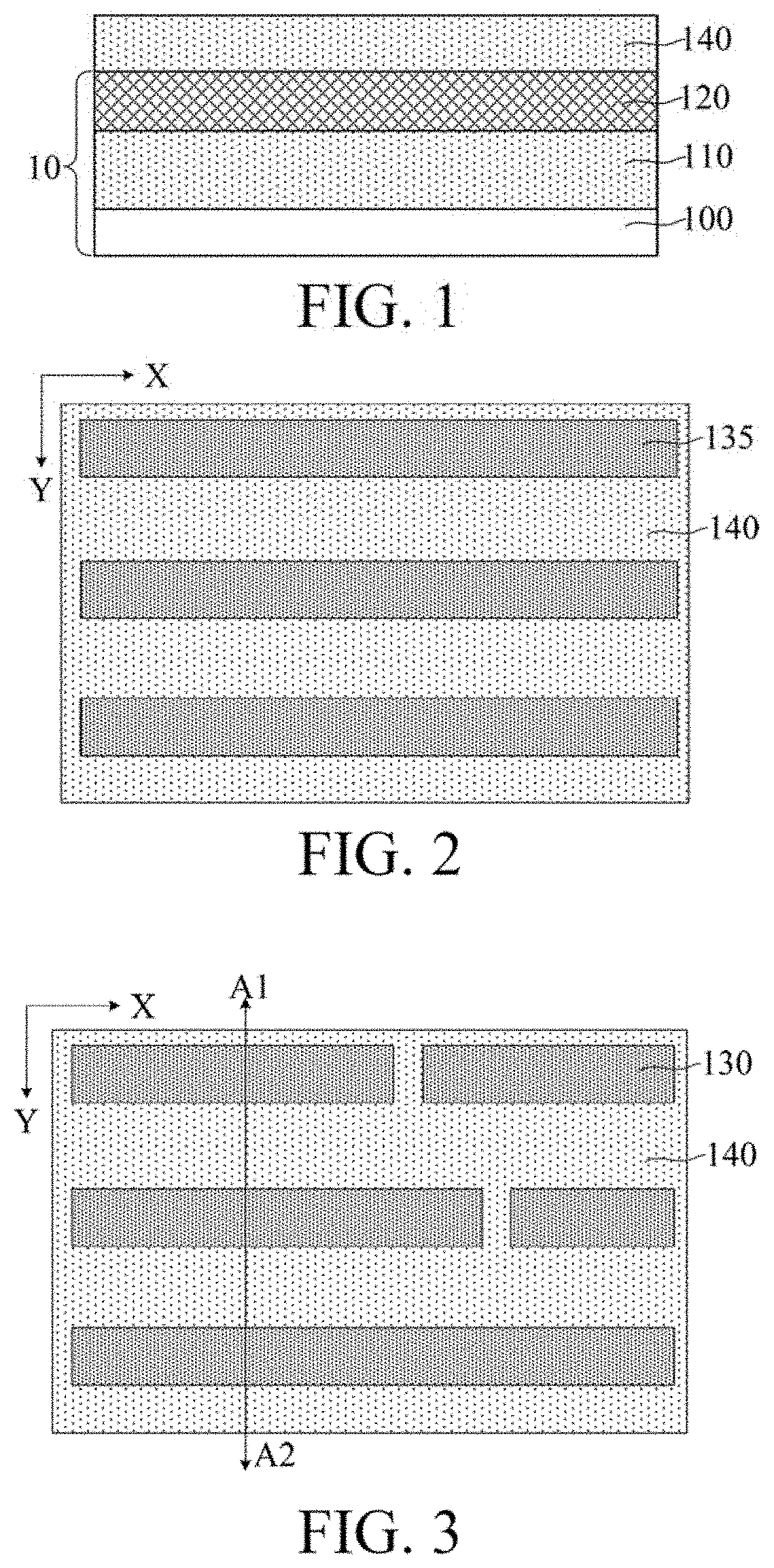
[0013]As can be known from the related art, as technological nodes become increasingly small, how to improve a matching degree between a target pattern formed on a wafer and a designed pattern has become a challenge.

[0014]It is found through research that a pitch between photoresist patterns keeps decreasing as the technological nodes become increasingly small. However, under the influence of a photolithography process, when a pitch between adjacent photolithographic patterns is less than a threshold distance of the photolithography process, the photoresist patterns tend to deform or distort. Correspondingly, when the photoresist patterns are transferred to a base to form a target pattern (for example, a trench), pattern accuracy of the target pattern is reduced, and the accuracy of pattern transfer is further reduced.

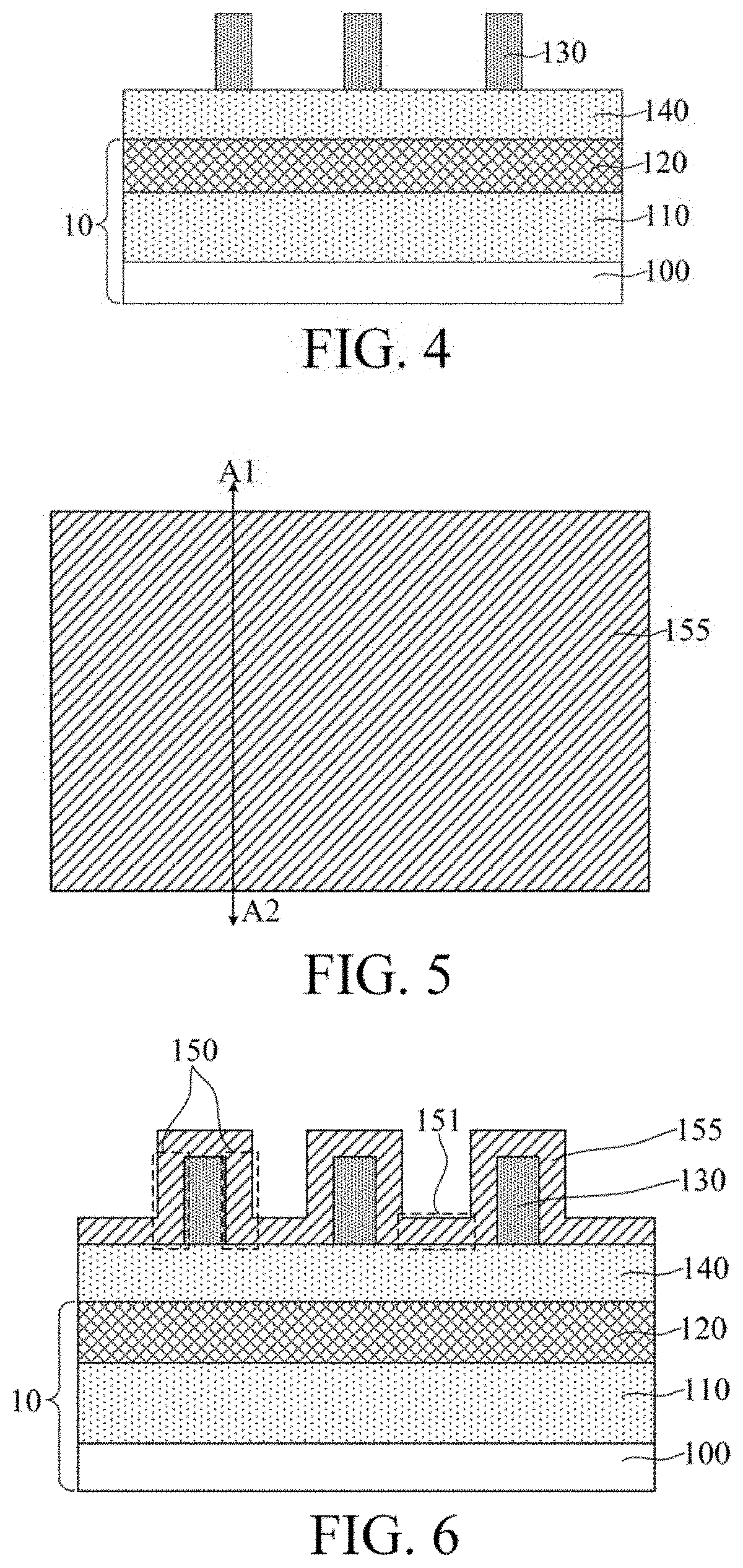
[0015]To address the technical problems, in embodiments and implementations of the present disclosure, a mandrel layer is formed on a base to occupy a position of a se...


PUM


Abstract

The present disclosure provides a semiconductor structure and a forming method thereof. One form of a forming method includes: providing a base; forming a plurality of discrete mandrel layers on the base, where an extending direction of the mandrel layers is a first direction, and a direction perpendicular to the first direction is a second direction; forming a plurality of spacer layers covering side walls of the mandrel layers; forming a pattern transfer layer on the base, where the pattern transfer layer covers side walls of the spacer layers; forming a first trench in the pattern transfer layer between adjacent spacer layers in the second direction; removing a mandrel layer to form a second trench after the first trench is formed; and etching the base along the first trench and the second trench to form a target pattern by using the pattern transfer layer and the spacer layer as a mask. In the present disclosure, the accuracy of the pattern transfer is improved.

Description

RELATED APPLICATIONS[0001]The present application claims priority to Chinese Patent Appln. No. 202010524386.1, filed Jun. 10, 2020, the entire disclosure of which is hereby incorporated by reference.BACKGROUNDTechnical Field[0002]Embodiments and implementations of the present disclosure relate to the field of semiconductor manufacturing, and in particular, to a semiconductor structure and a forming method thereof.Related Art[0003]With the rapid growth of the semiconductor integrated circuit (IC) industry, semiconductor technology continues to develop toward smaller process nodes driven by Moore's Law, so that ICs develop toward a direction of smaller size, higher circuit precision, and higher circuit complexity.[0004]In the development process of the ICs, generally, as a functional density (that is, a quantity of interconnection structures per chip) gradually increases, the geometric size (that is, the smallest component size that can be produced by using process steps) gradually de...

Claims


Application Information

Patent Timeline
IPC IPC(8): H01L21/033H01L21/311H01L21/768
CPCH01L21/0337H01L21/31144H01L21/31122H01L21/0332H01L21/31116H01L21/76816H01L23/528H01L21/823431H01L21/823475H01L27/0886H01L2221/101
Inventor CHEN, ZHUZUOPENG, HEMING, YANGDALIN, YAODUOHUI, BEI
Owner SEMICON MFG INT (SHANGHAI) CORP
Why Eureka
Try Eureka