Chip parts and method for manufacturing the same, circuit assembly having the chip parts and electronic device

a technology of chip parts and circuit assemblies, applied in semiconductor devices, semiconductor/solid-state device testing/measurement, semiconductor/solid-state device details, etc., can solve problems such as excessive effort and “defective” judgment, and achieve the effects of reducing productivity, improving inspection precision, and small siz

Active Publication Date: 2015-08-27
ROHM CO LTD
View PDF9 Cites 14 Cited by
  • Summary
  • Abstract
  • Description
  • Claims
  • Application Information

AI Technical Summary

Benefits of technology

[0007]To prevent such misrecognition, a detection system (part recognizing camera, etc.) and an illumination system (light source, etc.) of the automatic optical inspection machine must be optimized according to each inspection object to improve the inspection precision and thus extra effort is required for the appearance inspection and productivity is decreased. Moreover, such effort becomes excessive as chip parts of even smaller size become desired.
[0008]Therefore a

Problems solved by technology

However, a chip part is not necessarily mounted in a horizontal attitude onto a mounting substrate and there are cases where a chip part is mounted in an inclined attitude onto a mounting substrate.
This le

Method used


Image

  • Chip parts and method for manufacturing the same, circuit assembly having the chip parts and electronic device
  • Chip parts and method for manufacturing the same, circuit assembly having the chip parts and electronic device
  • Chip parts and method for manufacturing the same, circuit assembly having the chip parts and electronic device

Examples


first preferred embodiment

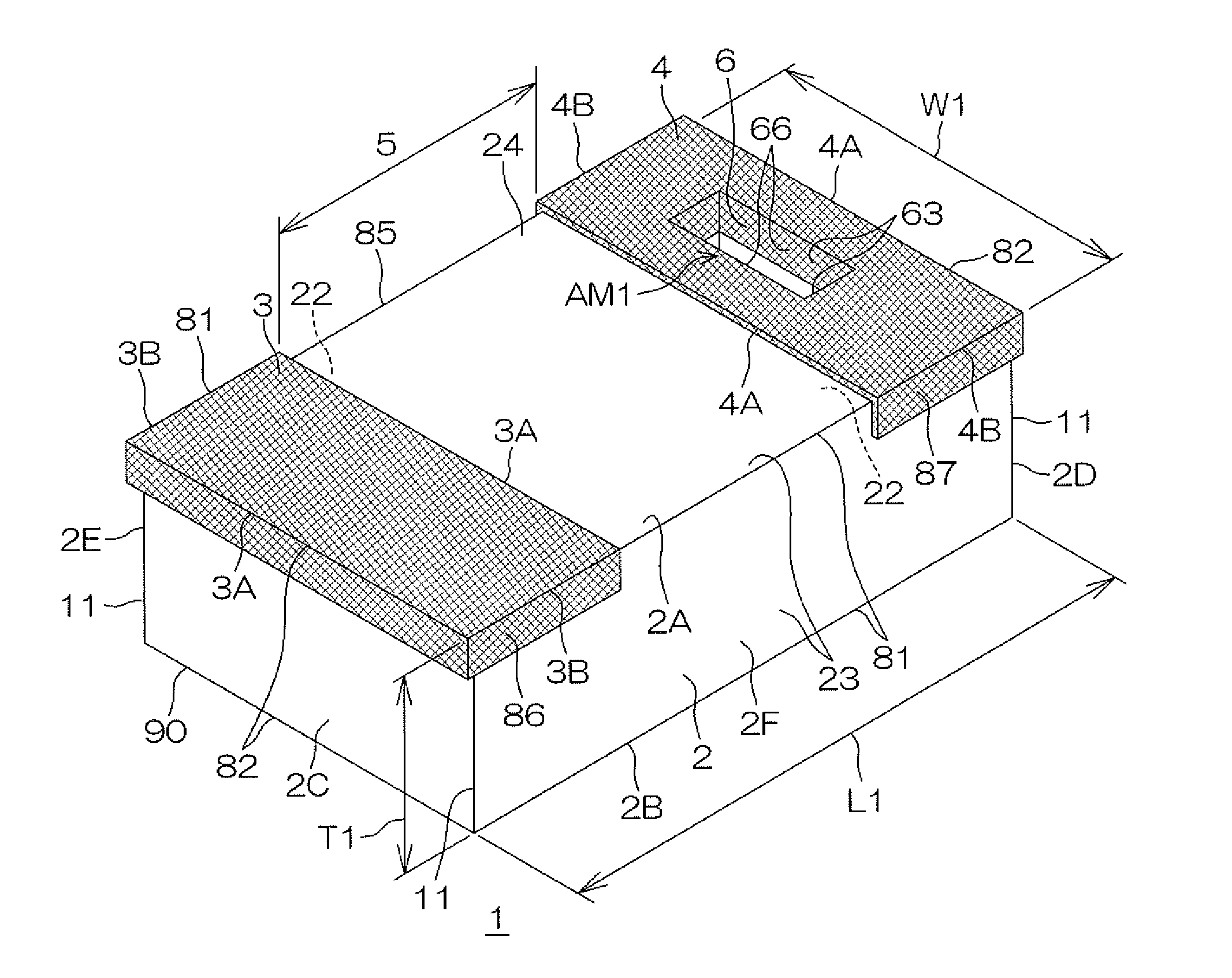
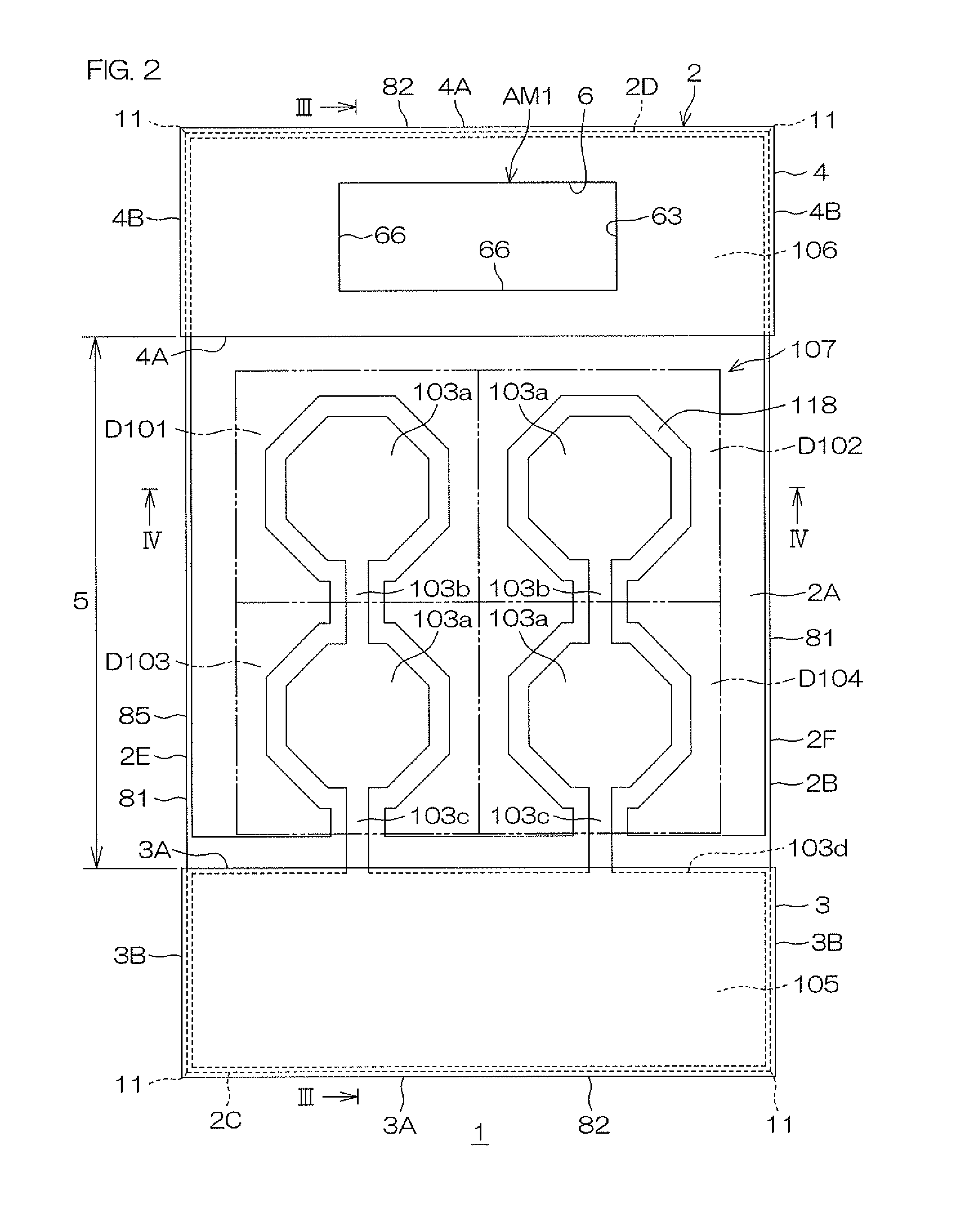
[0172]FIG. 1 is a schematic perspective view of a chip part 1 according to a first preferred embodiment of the present invention. For the sake of description, in FIG. 1, cross hatching is applied to first and second connection electrodes 3 and 4 to be described later.

[0173]The chip part 1 is a minute chip part and has a substantially rectangular parallelepiped shape as shown in FIG. 1. The planar shape of the chip part 1 may, for example, be a rectangle (0603 chip) with a length L1 along a long side 81 being not more than 0.6 mm and a length W1 along a short side 82 being not more than 0.3 mm or may be a rectangle (0402 chip) with the length L1 along the long side 81 being not more than 0.4 mm and the length W1 along the short side 82 being not more than 0.2 mm. More preferably, the dimension of the chip part 1 is a rectangle (03015 chip) with the length L1 along the long side 81 being 0.3 mm and the length W1 along the short side 82 being 0.15 mm. The chip part 1 has a thickness T1...

second preferred embodiment

[0264]FIG. 17 is a plan view for describing the arrangement of a chip part 201 according to a second preferred embodiment of the present invention. FIG. 18 is a sectional view taken along section line XVIII-XVIII shown in FIG. 17.

[0265]The chip part 201 includes the substrate 2, a cathode electrode film 233 and an anode electrode film 234 formed on the substrate 2, and a plurality of diode cells D201 to D204 connected in parallel between the cathode electrode film 233 and the anode electrode film 234. The substrate 2 has the penetrating hole 6 formed therein in the same arrangement as in the first preferred embodiment described above.

[0266]A cathode pad 235 and an anode pad 236 are respectively disposed at respective end portions in the long direction of the substrate 2. A diode cell region 237 of rectangular shape is set between the cathode pad 235 and the anode pad 236. The plurality of diode cells D201 to D204 are aligned two-dimensionally inside the diode cell region 237. In the...

third preferred embodiment

[0275]FIG. 19 is a plan view of a chip part 401 according to a third preferred embodiment of the present invention. FIG. 20 is a sectional view taken along section line XX-XX shown in FIG. 19. FIG. 21 is a sectional view taken along section line XXI-XXI shown in FIG. 19.

[0276]A point of difference of the chip part 401 according to the third preferred embodiment with respect to the chip part 1 according to the first preferred embodiment described above is that in place of the diode cells D101 to D104, first and second Zener diodes D401 and D402 are formed as the circuit elements formed in the element region 5. Arrangements of other portions are equivalent to the arrangements in the chip part 1 according to the first preferred embodiment. In FIG. 19 to FIG. 21, portions corresponding to the respective portions shown in FIG. 1 to FIG. 18 are provided with the same reference symbols.

[0277]The chip part 401 includes the substrate 2 (for example, a p+-type silicon substrate), the first Ze...


PUM


Abstract

A chip part according to the present invention includes a substrate having a penetrating hole, a pair of electrodes formed on a front surface of the substrate and including one electrode overlapping the penetrating hole in a plan view and another electrode facing the one electrode, and an element formed on the front surface side of the substrate and electrically connected to the pair of electrodes.

Description

CROSS-REFERENCE TO RELATED APPLICATIONS[0001]The present application corresponds to Japanese Patent Application No. 2014-1910 filed in the Japan Patent Office on Jan. 8, 2014, Japanese Patent Application No. 2014-1911 filed in the Japan Patent Office on Jan. 8, 2014, Japanese Patent Application No. 2014-17689 filed in the Japan Patent Office on Jan. 31, 2014, and Japanese Patent Application No. 2014-220433 filed in the Japan Patent Office on Oct. 29, 2014, and all the disclosures of the applications will be incorporated herein by citation.FIELD OF THE INVENTION[0002]The present invention relates to a chip part, a method for manufacturing the chip part, and a circuit assembly and an electronic device that include the chip part.BACKGROUND ART[0003]Patent Document 1 (Japanese Patent Application Publication No. 8-316001) discloses a chip type electronic part including a pair of electrodes formed on an insulating substrate, an element formed between the pair of electrodes, an overcoat la...

Claims


Application Information

Patent Timeline
IPC IPC(8): H01L23/00
CPCH01L24/06H01L24/03H01L2224/03464H01L2224/05551H01L2224/03602H01L2224/04026H01L21/6836H01L21/78H01L22/12H01L23/4824H01L23/544H01L24/05H01L24/29H01L24/32H01L29/0619H01L29/8611H01L29/866H01L29/872H01L2221/68313H01L2221/68327H01L2221/6834H01L2221/68381H01L2223/54413H01L2223/5442H01L2223/54433H01L2223/54486H01L2224/05017H01L2224/0502H01L2224/05023H01L2224/05552H01L2224/05557H01L2224/0556H01L2224/05562H01L2224/05567H01L2224/05568H01L2224/05582H01L2224/05644H01L2224/06051H01L2224/06151H01L2224/32013H01L2224/32054H01L2224/32057H01L2224/32105H01L2224/32237H01L2224/33151H01L2224/75745H01L2224/75753H01L2224/83192H01L2224/83815H01L2224/94H01L2924/10156H01L2924/12035H01L2924/12036H01L2924/12042H01L2924/00H01L2924/00012H01L2924/00014H01L2224/03
Inventor YAMAMOTO, HIROKI
Owner ROHM CO LTD
Why Eureka
Try Eureka