Liquid crystal display device and display control method thereof

a liquid crystal display device and control method technology, applied in static indicating devices, non-linear optics, instruments, etc., can solve the problems of easy generation of color shift problems, channel its width cannot be infinitely small, so as to increase the aperture of the liquid crystal display device, reduce the preset channel width, and increase the pixel

Active Publication Date: 2015-09-03
SHENZHEN CHINA STAR OPTOELECTRONICS TECH CO LTD
View PDF4 Cites 5 Cited by
  • Summary
  • Abstract
  • Description
  • Claims
  • Application Information

AI Technical Summary

Benefits of technology

[0023]The beneficial effects of the present invention are: the liquid crystal display device of the present invention, through disposing each sub-pixel unit includes multiple display regions and multiple control switches, wherein the multiple control switches comprises a first control switch set and a second control switch set, and the first control switch set and the second control switch set are connected in parallel with the same data line such that when applying the corresponding data voltages to the multiple display regions through the data line, a voltage sum of the first control switch set is equal to a voltage sum of the second control switch set. Therefore, comparing to the conventional art with one of the control switch sets, the preset channel width is greatly reduced, and overall speaking, a sum of the areas occupied by the multiple control switches is reduced, which can increase the pixel, aperture of the liquid crystal display device with wide viewing angle and decrease the power consumption.

Problems solved by technology

Especially, in the application of large-size liquid crystal display device, it requires having a wider range of viewing angles, and the wide viewing angle liquid crystal display device easily generates the color shift problem when displaying.
Because of the limitation of the TFT fabrication process, the channel width cannot be infinitely small.
Because of the limitation of the TFT fabrication process, its width cannot be infinitely small.

Method used


Image

  • Liquid crystal display device and display control method thereof
  • Liquid crystal display device and display control method thereof
  • Liquid crystal display device and display control method thereof

Examples


second embodiment

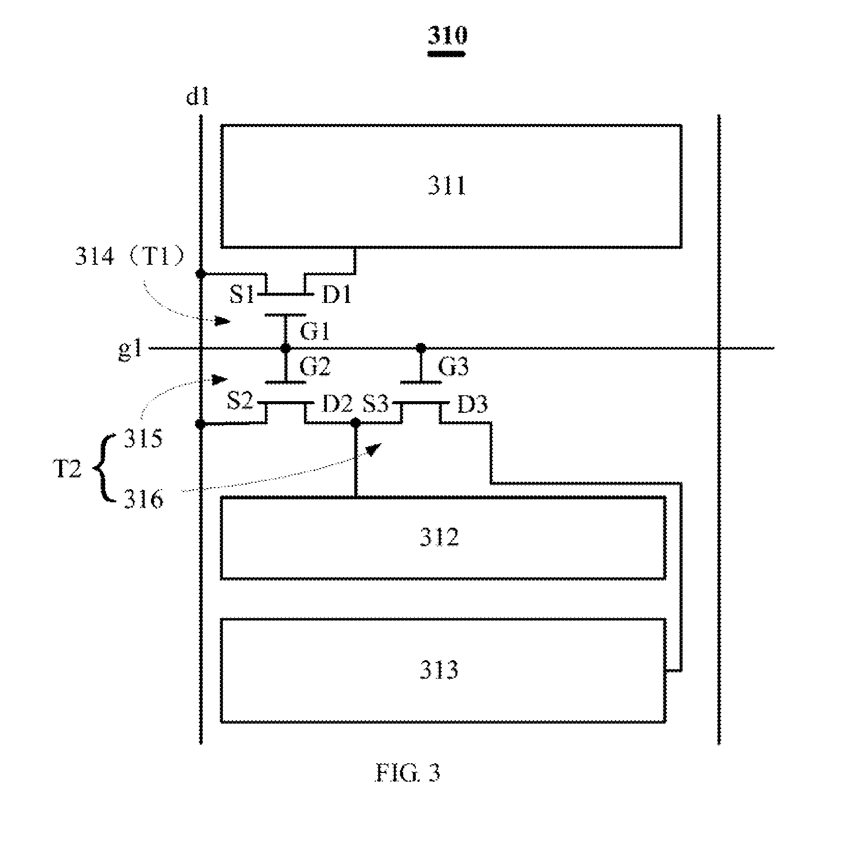
[0038]FIG. 4 is a schematic equivalent circuit of a sub-pixel unit according to the present invention. As shown in FIG. 4, a sub-pixel unit 510 of this embodiment further includes a common electrode line c1, which is based on the embodiment shown in FIG. 3, and further includes a fourth transistor 517.

[0039]Wherein, a source electrode S4 of the fourth transistor 517 is connected with the drain electrode D3 of the third transistor 516 (corresponds to the third transistor 316 shown in FIG. 3). The drain electrode D4 connects with the common electrode line c1, and a gate electrode G4 connects with the scan line g1.

[0040]When distribute the voltages applied at the second display region 512 and the third display region 513, the fourth transistor 517 mainly used for voltage dividing. And when the data line d1 stop providing power to the second transistor 515 and the third transistor 516, the fourth transistor 517 can prevent the voltage at the common electrode c1 from returning in order t...

third embodiment

[0041]It should be understood that in the present invention, it can dispose a first transistor 614 (corresponds to the first transistor 314 shown in FIG. 3) and connected in series with a fourth transistor 617 based on the embodiment shown in FIG. 3 to form a sub-pixel unit 610 as shown in FIG. 5, wherein the sub-pixel unit 610 further includes the common electrode line c1.

[0042]Wherein, the source electrode S4 of the fourth transistor 617 connects with a drain electrode D1 of the first transistor 614 and the drain electrode D4 connects with the common electrode line c1. The gate electrode G4 connects with the scan line g1. In this embodiment, the fourth transistor 617 mainly functions as voltage dividing and prevents the current from flowing back.

fourth embodiment

[0043]In the present invention, it can dispose a first transistor 714 (corresponds to the first transistor 314 shown in FIG. 3) to connect in series with a fourth transistor 717 based on the embodiment shown in FIG. 3. At the same time, a third transistor 716 (corresponds to the third transistor 316 shown in FIG. 3) connects in series with a fifth transistor 718 to form a sub-pixel unit 710 shown in FIG. 6, wherein the sub-pixel unit 710 further includes the common electrode line c1.

[0044]Wherein a source electrode S4 of the fourth transistor 717 connects with a drain electrode D1 of the first transistor 714 and the drain electrode D4 connects with the common electrode line c1 A gate electrode 04 connects with the scan line g1. A source electrode 55 of the fifth transistor 718 connects with the drain electrode D3 of the third transistor 716. A drain electrode D5 connects with the common electrode line c1. The gate electrode G5 connects with the scan line g1. In this embodiment, the ...


PUM


Abstract

The present invention provides a liquid crystal display device and display control method thereof Each sub-pixel of the liquid crystal display device includes multiple display regions and multiple control switches for controlling the display regions to receive corresponding data voltages, wherein, the multiple control switches includes a first control switch set and a second control switch set, and the first control switch set and the second control switch set are connected in parallel with the same data line. Through the above way, the present invention can increase the pixel aperture ratio of the wide-viewing-angle liquid crystal display device and decrease the power consumption.

Description

BACKGROUND OF THE INVENTION[0001]1. Field of the Invention[0002]The present invention relates to the field of the display technology, and more particularly to a liquid crystal display device and a display control method thereof.[0003]2. Description of Related Art[0004]The liquid crystal display (LCD) market are growing rapidly and expanding its field of application continuously. Especially, in the application of large-size liquid crystal display device, it requires having a wider range of viewing angles, and the wide viewing angle liquid crystal display device easily generates the color shift problem when displaying.[0005]In order to solve the color shift problem, the prior art mainly disposes multiple display regions for each sub-pixel unit, such as shown in FIG. 1. A sub-pixel unit 100 includes three display regions 110, 120, 130. With reference to FIG. 1, three transistors 111, 121, 131 corresponding to the three display regions 110, 120, 130 are connected in series with a data l...

Claims


Application Information

Patent Timeline
Patent Type & Authority Applications(United States)
IPC IPC(8): G09G3/36
CPCG09G3/3607G09G2300/0447G09G3/3696G02F1/13624G02F2201/40G02F1/134345G02F1/1362
Inventor CHEN, CHENG-HUNGLIAO, ZUOMIN
Owner SHENZHEN CHINA STAR OPTOELECTRONICS TECH CO LTD
Why Eureka
Try Eureka