Supercharge Your Innovation With Domain-Expert AI Agents!

Fault analysis apparatus and fault analysis method

a fault analysis and fault technology, applied in the field of fault analysis apparatus and fault analysis method for semiconductors, can solve the problems of difficult to specify the defective part from differences in measured values, and the defective part in the wiring area is difficult to become continuous irradiation positions, so as to simplify the measurement, reduce the measurement time, and simplify the effect of measuremen

Active Publication Date: 2015-09-10
HAMAMATSU PHOTONICS KK
View PDF10 Cites 9 Cited by
  • Summary
  • Abstract
  • Description
  • Claims
  • Application Information

AI Technical Summary

Benefits of technology

This patent describes a fault analysis apparatus for semiconductor devices that uses light irradiation to detect defects in the wiring area. The apparatus uses a scan direction to access the wiring areas, which intersects with the wiring directions at an angle. This angle prevents the scan direction from being parallel to the wiring directions, making it difficult for defects to become continuous irradiation positions. This simplifies the measurement process and reduces the time required for analysis. The apparatus also creates a two-dimensional map of the semiconductor device by performing a coordinate transformation that takes account of the scan direction to make it easier to specify faults. Additionally, the map creation unit may superimpose an image of the light irradiation position and measured value onto an image of the semiconductor device structure to further aid in identifying the fault.

Problems solved by technology

This makes it difficult to specify the defective part from differences in measured values.
As a consequence, when there is a defective part in the wiring area, for example, the other part in the wiring area and the defective part in the wiring area are hard to become continuous irradiation positions.

Method used


Image

  • Fault analysis apparatus and fault analysis method
  • Fault analysis apparatus and fault analysis method
  • Fault analysis apparatus and fault analysis method

Examples


first embodiment

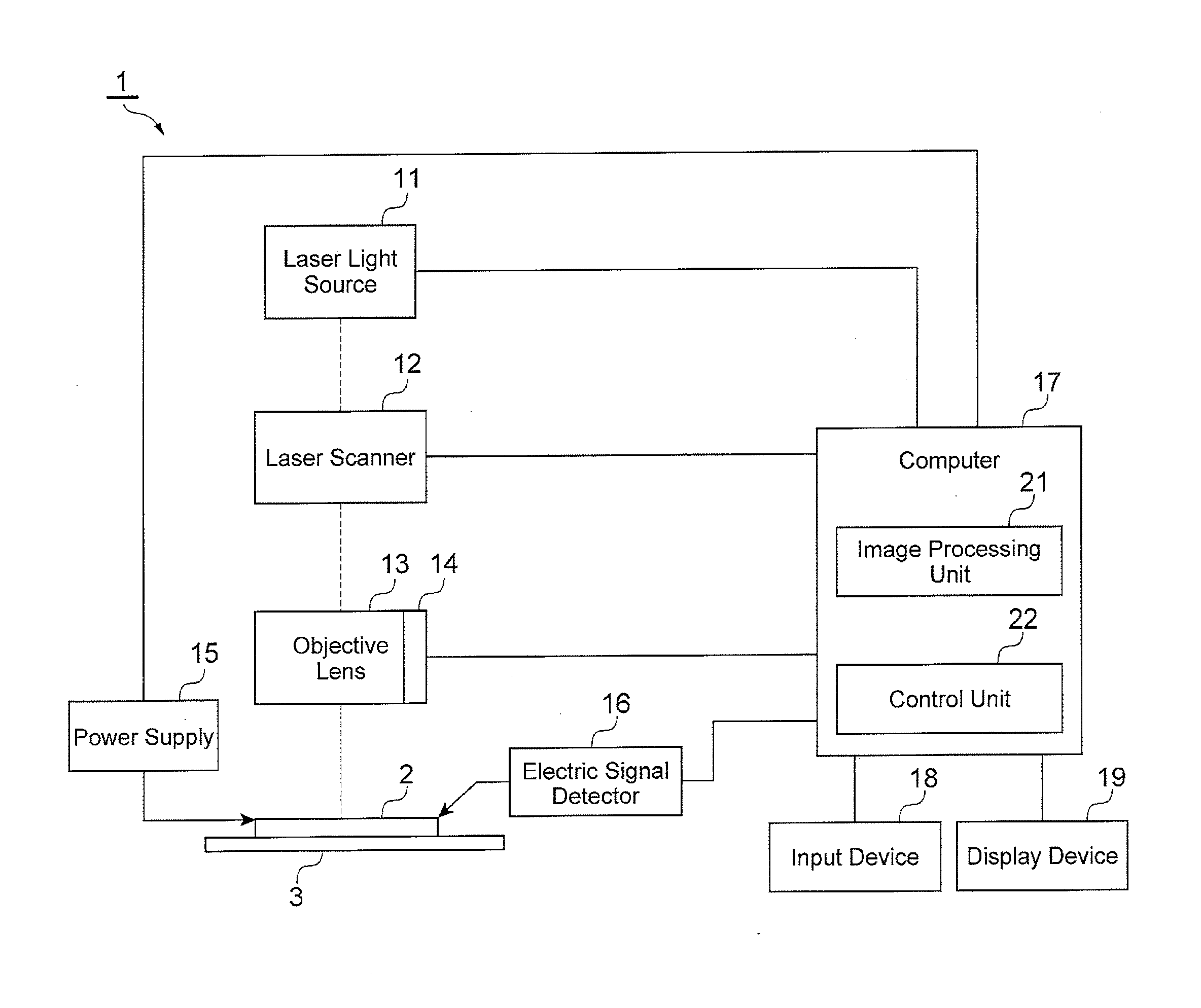
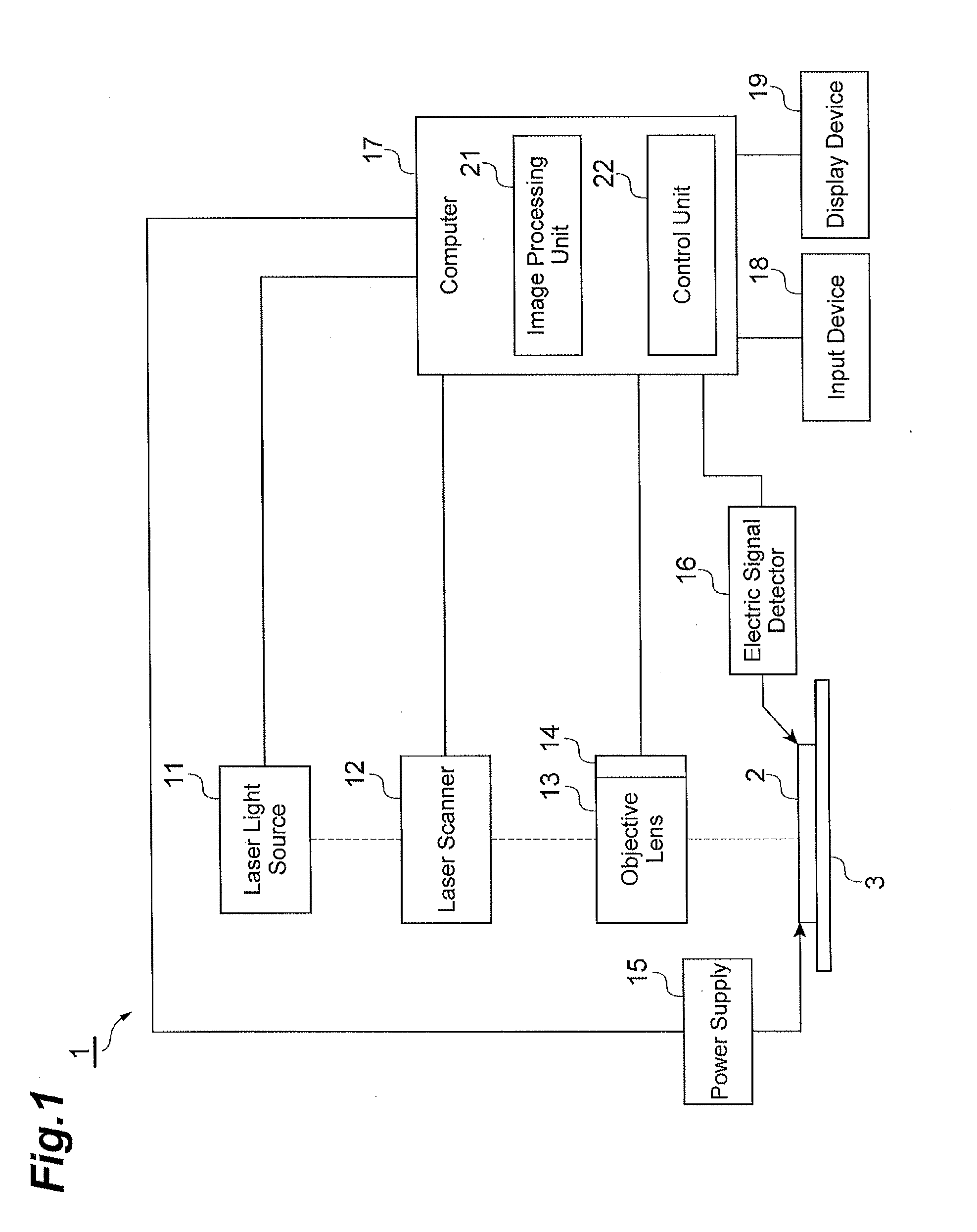
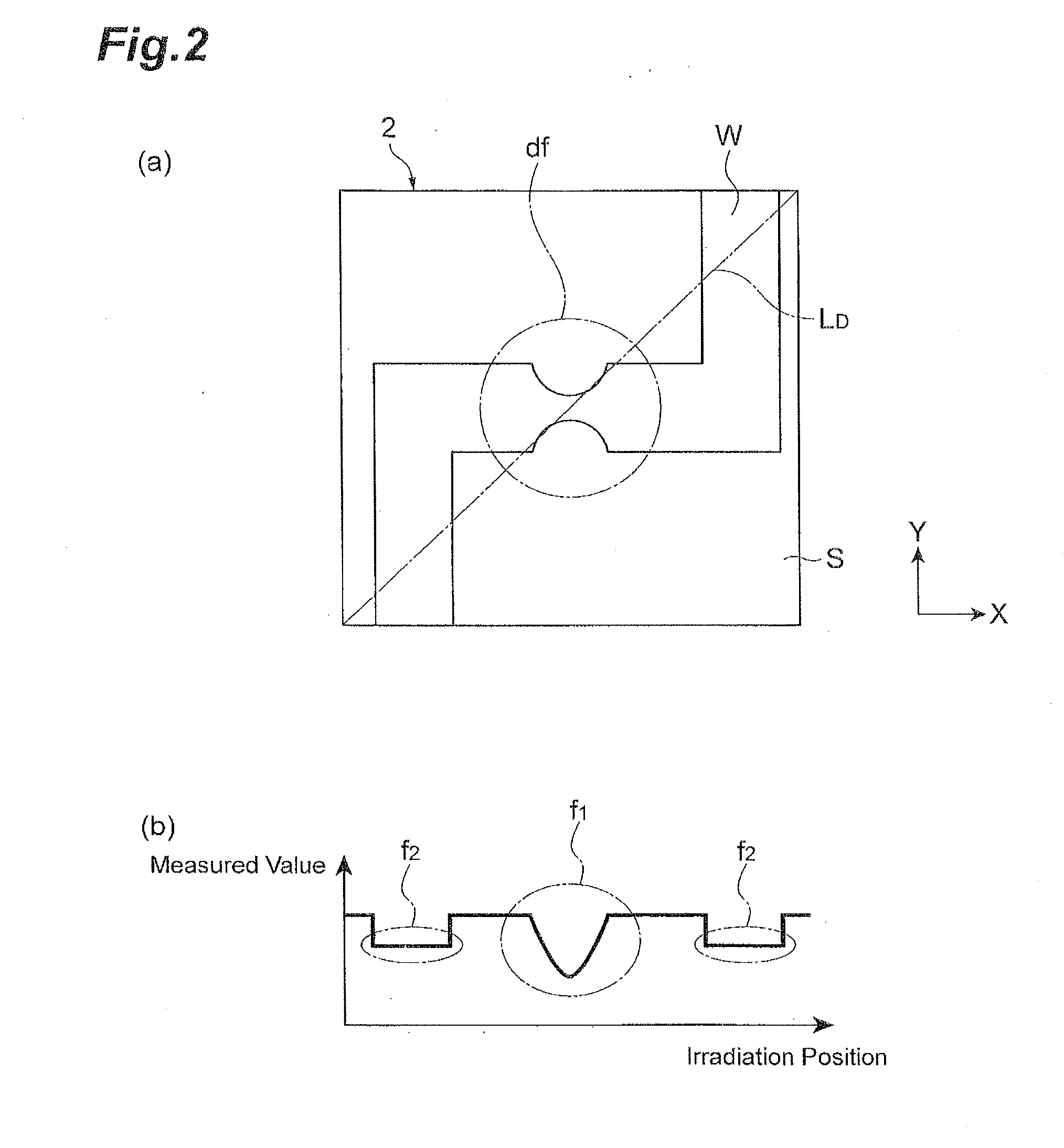
[0025]FIG. 1 is a structural diagram of the fault analysis apparatus in accordance with the first embodiment of the present invention. As illustrated in FIG. 1, the fault analysis apparatus 1 in accordance with the first embodiment is an apparatus for inspecting a semiconductor device 2, which is a device under test (DUT), by specifying a location where an abnormality occurs therein, for example. Specifically, the fault analysis apparatus 1 is an apparatus for measuring a reaction of the semiconductor device 2 by irradiating the semiconductor device 2 with light.

[0026]The fault analysis apparatus 1 is a fault analysis apparatus for analyzing a fault by OBIRCH or OBIC measurement. The OBIRCH measurement is a technique for measuring a change in resistance value accompanying heat or the like generated when the semiconductor device is irradiated with laser light. The OBIC measurement is a technique for measuring a photovoltaic current generated when the semiconductor device is irradiate...

second embodiment

[0051]A fault analysis apparatus IA in accordance with the second embodiment will now be explained in detail with reference to FIG. 7. FIG. 7 is a structural diagram of the fault analysis apparatus 1A in accordance with the second embodiment. In this embodiment, differences from the former embodiment will mainly be explained.

[0052]The fault analysis apparatus 1A is a fault analysis apparatus for analyzing a fault by DALS measurement. The DALS measurement is a technique which measures a reaction of a semiconductor device irradiated with laser light while a test pattern is inputted to the semiconductor device. As illustrated in FIG. 7, the fault analysis apparatus 1A in accordance with this embodiment uses a tester 31 as a measurement unit in place of the electric signal detector 16 in the fault analysis apparatus 1. The tester 31 feeds the semiconductor device 2 with an operation pulse signal (test pattern) corresponding to a predetermined driving action. When fed with the test patte...


PUM

PropertyMeasurementUnit
angleaaaaaaaaaa
angleaaaaaaaaaa
angleaaaaaaaaaa

Abstract

A fault analysis apparatus is an apparatus for measuring a reaction of a semiconductor device having a wiring extending in two directions orthogonal to each other. The fault analysis apparatus comprises a laser light source that outputs laser light, a control unit that sets a scan direction which is a direction of scanning an irradiation position of the laser light in the semiconductor device, a laser scanner that scans the laser light according to the scan direction, an electric signal detector that measures the reaction of the semiconductor device to the laser light and outputs a measured value, and an image processing unit that creates a two-dimensional map according to the irradiation position and the measured value. The control unit sets the scan direction such that the scan direction intersects the wiring extending directions at an angle greater than 0° but smaller than 90°.

Description

BACKGROUND OF THE INVENTION[0001]1. Field of the Invention[0002]The present invention relates to a fault analysis apparatus and a fault analysis method for a semiconductor.[0003]2.Related Background Art[0004]As a method for analyzing a fault of a semiconductor device, a method is known, in which laser light is irradiated to the semiconductor device so as to extract an electric signal from the semiconductor device, thereby analyzing the fault. Examples of such a method include OBIRCH (Optical Beam Induced Resistance Change) measurement which measures a change in resistance value accompanying heat caused by irradiation with laser light or the like (see U.S. Pat. No. 6,320,396), OBIC (Optical Beam Induced Current) measurement which measures a photovoltaic current generated by irradiation with laser light, and DALS (Dynamic Analysis by Laser Stimulation) which measures a reaction to a stimulation caused by laser light in a state where a test pattern is inputted to the semiconductor devi...

Claims


Application Information

Patent Timeline
Patent Type & Authority Applications(United States)
IPC IPC(8): G01N21/17
CPCG01N21/17G01R31/311G01N21/00G01N21/84G01R31/28G01R31/302
Inventor KANEOKA, TAKAYOSHI
Owner HAMAMATSU PHOTONICS KK
Features
  • R&D
  • Intellectual Property
  • Life Sciences
  • Materials
  • Tech Scout
  • Unparalleled Data Quality
  • Higher Quality Content
  • 60% Fewer Hallucinations
Learn More