Semiconductor device having a gap defined therein

a technology of a semiconductor device and a gap is applied in the field of semiconductor devices having a gap defined therein, which can solve the problems of limiting the alternating current performance of the finfet device, the shape of the fin may limit the drive strength, and the finfet to a relatively low level, so as to reduce reduce the parasitic capacitance , the effect of reducing the delay time of the finfet transistor

Active Publication Date: 2015-09-10
QUALCOMM INC
View PDF3 Cites 51 Cited by
  • Summary
  • Abstract
  • Description
  • Claims
  • Application Information

AI Technical Summary

Benefits of technology

[0005]The present disclosure provides a semiconductor device having a gap (e.g., an air gap and / or a vacuum gap) defined therein. For example, a source / drain region of the semiconductor device may define the gap. A method of forming the semiconductor device, such as a FinFET device, may include depositing a first spacer material on a dummy gate (e.g., a sidewall of the dummy gate) of the semiconductor device. The method may also include depositing a sacrificial spacer on the first spacer material and depositing a second spacer material on the sacrificial spacer. The second spacer material may be in contact with the first spacer material. The method may further include removing the sacrificial spacer between the first spacer material and the second spacer material to create a cavity (having an opening) between the first spacer material and the second spacer material. For example, the sacrificial spacer material may be removed (e.g., etched) through the opening. The method may include filling the opening to establish a gap that is defined by a portion of the first spacer material and by a portion of the second spacer material. The opening may be filled (e.g., closed) with a third spacer material (e.g., a spacer cap) or a source / drain region material. The gap may be defined by a source / drain region of the semiconductor device. Additionally, the gap may be defined by the first spacer material, the second spacer material, the third spacer material, a substrate (e.g., a fin) of the semiconductor device, or a combination thereof, as illustrative, non-limiting examples. A height of the gap may be less than a height of a gate of the semiconductor device. The gap may enable a reduced parasitic capacitance and may increase a drive strength of the semiconductor device as compared to semiconductor devices that do not include a gap.
[0010]One particular advantage provided by at least one of the disclosed embodiments is reduced parasitic capacitance (e.g., a gate capacitance) and an AC performance improvement as compared to devices (e.g., FinFETs) that do not have a defined gap. Another particular advantage provided by at least one of the disclosed embodiments is that a FinFET transistor delay time may be reduced and / or a switch energy may be reduced as compared to FinFET devices that do not have a defined gap.

Problems solved by technology

When a FinFET device includes a single fin, a shape of the fin may limit a drive strength (e.g., a current, such as an alternating current) of the FinFET to a relatively low level.
However, the multiple fins may introduce parasitic capacitances that restrict (e.g., limit) alternating current performance of the FinFET device.

Method used


Image

  • Semiconductor device having a gap defined therein
  • Semiconductor device having a gap defined therein
  • Semiconductor device having a gap defined therein

Examples


Embodiment Construction

[0052]Particular embodiments of the present disclosure are described below with reference to the drawings. In the description, common features are designated by common reference numbers throughout the drawings.

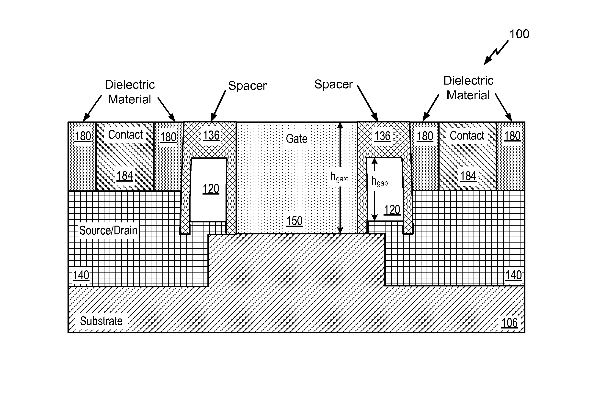
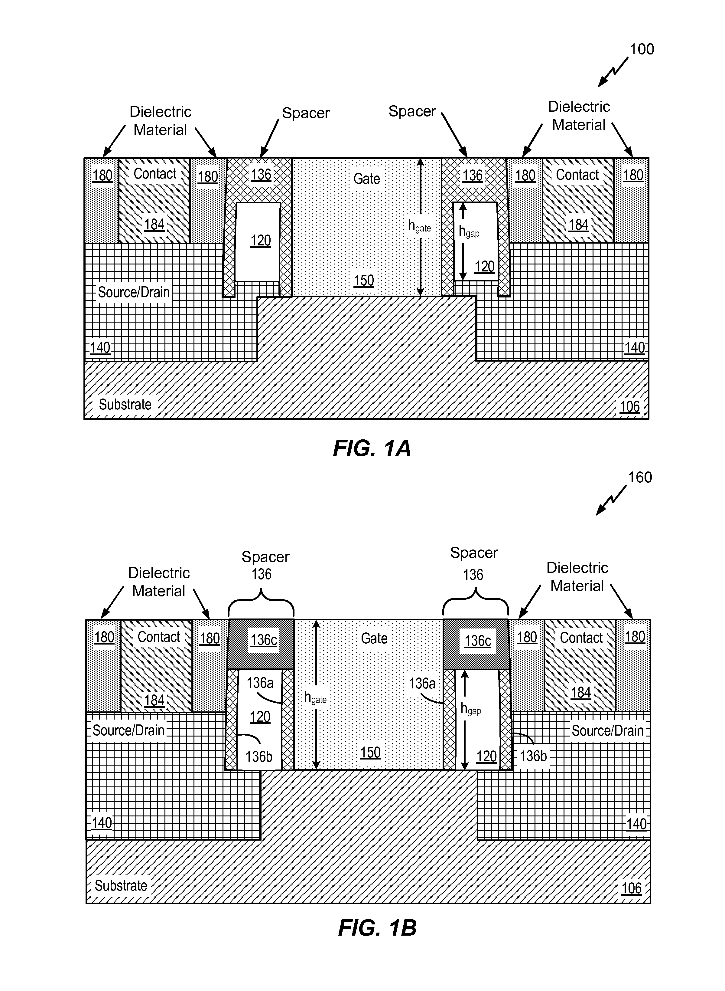
[0053]Referring to FIG. 1A, a diagram of a semiconductor device 100 having a gap defined therein is shown. The semiconductor device 100 may include or correspond to a field-effect transistor (FET) device, such as a FinFET device that includes one or more fins, a metal-oxide semiconductor (MOS) device, such as p-type metal-oxide-semiconductor (pMOS) device or an n-type metal-oxide-semiconductor (nMOS) device, as illustrative, non-limiting examples.

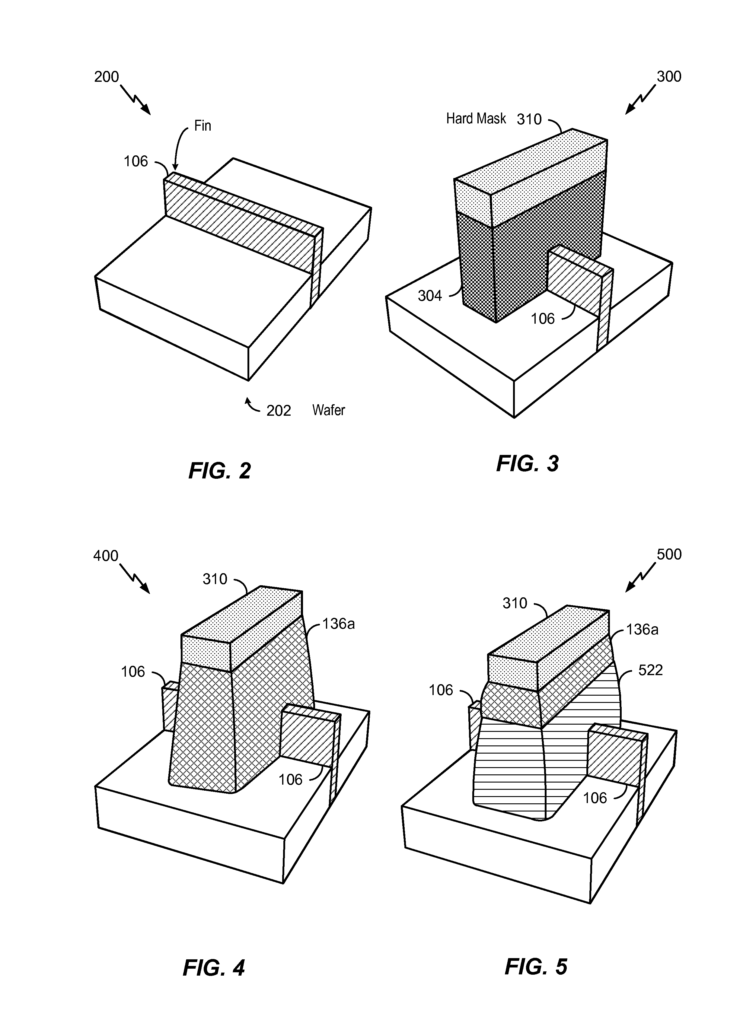
[0054]The semiconductor device 100 may include a substrate 106, one or more source / drain regions 140, dielectric material 180 (e.g. a dielectric layer), one or more contacts 184, a spacer 136, and a gate 150. The substrate 106 may be associated with and / or formed from a wafer, such as a silicon wafer, as an illustrative, non-limiting ...


PUM


Abstract

In a particular embodiment, a method includes forming a first spacer structure on a dummy gate of a semiconductor device and forming a sacrificial spacer on the first spacer structure. The method also includes etching a structure of the semiconductor device to create an opening, removing the sacrificial spacer via the opening, and depositing a material to close to define a gap.

Description

I. CROSS-REFERENCE TO RELATED APPLICATIONS[0001]The present application claims priority from commonly owned U.S. Provisional Pat. App. No. 61 / 950,681 filed Mar. 10, 2014 and entitled “SEMICONDUCTOR DEVICE HAVING A GAP DEFINED THEREIN” (Atty. Dkt. No. 141895P1), the contents of which are expressly incorporated herein by reference in their entiretyII. FIELD[0002]The present disclosure is generally related to a semiconductor device having a gap defined therein.III. DESCRIPTION OF RELATED ART[0003]Advances in technology have resulted in smaller apparatuses and more powerful computing devices. For example, there currently exist a variety of portable personal computing devices, including wireless computing devices, such as portable wireless telephones, personal digital assistants (PDAs), and paging devices that are small, lightweight, and easily carried by users. More specifically, portable wireless telephones, such as cellular telephones and internet protocol (IP) telephones, can communi...

Claims


Application Information

Patent Timeline
Patent Type & Authority Applications(United States)
IPC IPC(8): H01L29/66H01L29/78
CPCH01L29/6681H01L29/785H01L29/66545H01L29/4991H01L29/6653H01L29/66795
Inventor XU, JEFFREY JUNHAORIM, KERNZHU, JOHN JIANHONGSONG, STANLEY SEUNGCHULBADAROGLU, MUSTAFAMACHKAOUTSAN, VLADIMIRYANG, DAYEAP, CHOH FEI
Owner QUALCOMM INC
Why Eureka
Try Eureka