Making multi-layer micro-wire structure

a micro-wire and structure technology, applied in the field of substrate structures, can solve the problems of limited transparency and conductivity, tendency to crack under mechanical or environmental stress, and increasing cost of transparent conductive metal oxides, and achieve the effect of fewer manufacturing steps

Inactive Publication Date: 2015-09-24
EASTMAN KODAK CO
View PDF5 Cites 14 Cited by
  • Summary
  • Abstract
  • Description
  • Claims
  • Application Information

AI Technical Summary

Benefits of technology

[0021]The present invention provides a multi-layer micro-wire structure, a multi-area micro-wire structure, and a method of making a multi-layer micro-wire structure with fewer manufacturing steps.

Problems solved by technology

Transparent conductive metal oxides are well known in the display and touch-screen industries and have a number of disadvantages, including limited transparency and conductivity and a tendency to crack under mechanical or environmental stress.
Transparent conductive metal oxides are increasingly expensive and relatively costly to deposit and pattern.
Moreover, the substrate materials are limited by the electrode material deposition process (e.g. sputtering) and the current-carrying capacity of such electrodes is limited, thereby limiting the amount of power that is supplied to the pixel elements.
Although thicker layers of metal oxides or metals increase conductivity, they also reduce the transparency of the electrodes.

Method used


Image

  • Making multi-layer micro-wire structure
  • Making multi-layer micro-wire structure
  • Making multi-layer micro-wire structure

Examples


Embodiment Construction

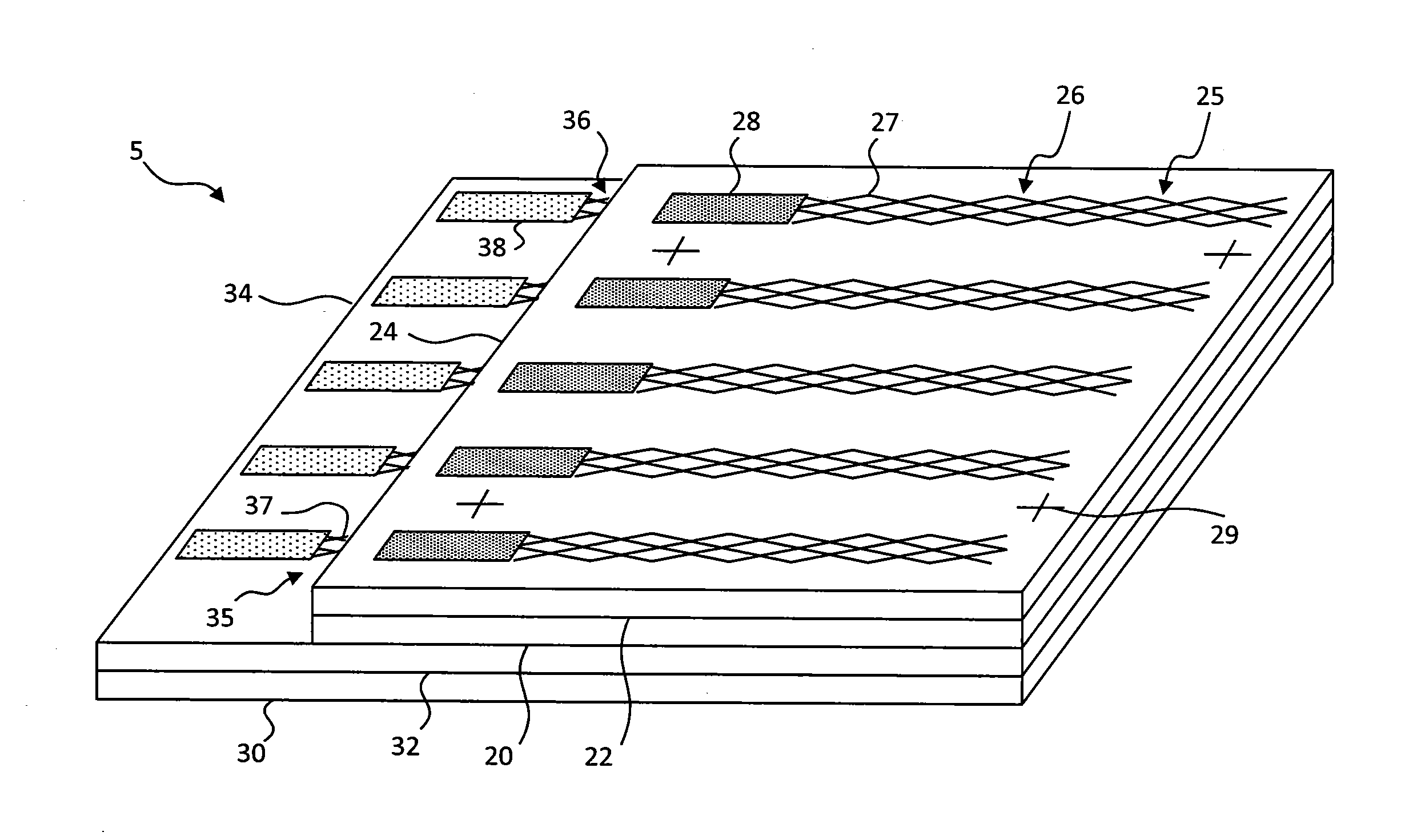
[0039]The present invention is directed toward multi-layer and multi-area micro-wire structures and methods of making such structures with improved efficiency and reduced cost. In an embodiment, the multi-layer micro-wire structure is used in a capacitive touch screen or in conjunction with a display device.

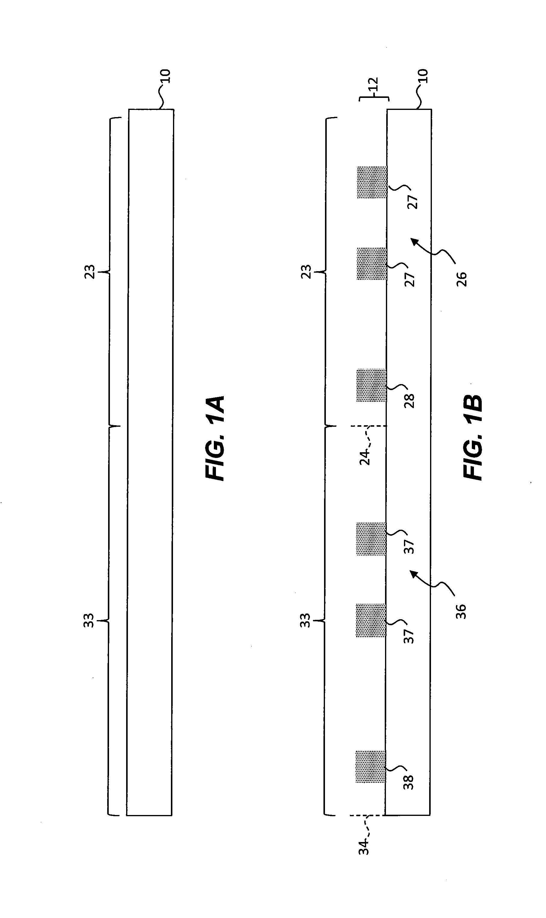
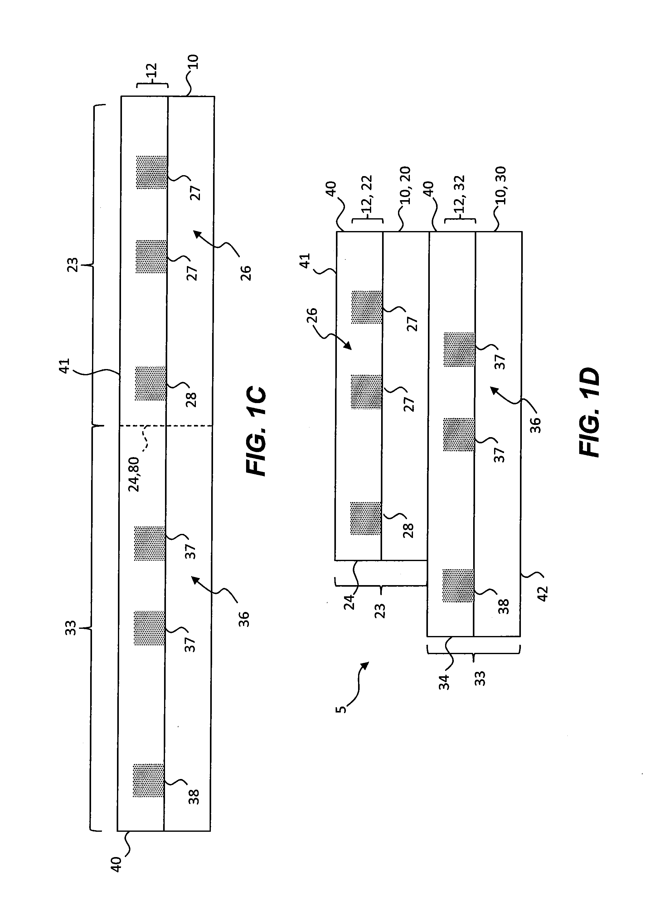
[0040]Referring to the cross sections of FIGS. 1A-1D and to the flow diagram of FIG. 2, in an embodiment of the present invention a method of making a multi-layer micro-wire structure 5 (FIG. 1D) includes providing a substrate 10 having first and second distinct and separated areas 23, 33 (FIG. 1A) in step 200. Referring to FIG. 1B, a micro-wire layer 12 is located in contact with the substrate 10 in step 210. The micro-wire layer 12 has a first layer edge 24 and a second layer edge 34 different from the first layer edge 24. The micro-wire layer 12 also has first and second distinct and separated areas 23, 33 spatially corresponding to the first and second distinct and separated ...


PUM

PropertyMeasurementUnit
transparencyaaaaaaaaaa

Abstract

A method of making a multi-layer micro-wire structure includes providing a substrate with a micro-wire layer having first and second areas. The micro-wire layer includes first and second micro-wire electrodes and first and second connection pads in the first and second areas, respectively. Each micro-wire electrode includes one or more electrically connected micro-wires and is electrically connected to a connection pad. The micro-wires are located in a common step. The first area is separated from the second area and the first area of the substrate and the second area of the micro-wire layer are located between the first micro-wires and the second area of the substrate so that a second layer edge extends at least partly beyond a first layer edge and one or more of the second connection pads is located between at least a portion of the first layer edge and the second layer edge.

Description

CROSS REFERENCE TO RELATED APPLICATIONS[0001]Reference is made to commonly-assigned, co-pending U.S. patent application Ser. No. ______ (Kodak Docket K001745) filed concurrently herewith, entitled “Multi-Layer Micro-Wire Structure” by Ronald S. Cok, and commonly-assigned, co-pending U.S. patent application Ser. No. ______ (Kodak Docket K001746) filed concurrently herewith, entitled “Multi-Area Micro-Wire Structure” by Ronald S. Cok, the disclosures of which are incorporated herein.[0002]Reference is made to commonly-assigned, co-pending U.S. patent application Ser. No. 14 / 023,740, filed Sep. 11, 2013, entitled “Multi-Layer Micro-Wire Substrate Structure” by Ronald S. Cok and to commonly-assigned, co-pending U.S. patent application Ser. No. 14 / 023,757, filed Sep. 11, 2013, entitled “Multi-Layer Micro-Wire Substrate Method” by Ronald S. Cok, the disclosures of which are incorporated herein.FIELD OF THE INVENTION[0003]The present invention relates to substrate structures and methods fo...

Claims


Application Information

Patent Timeline
Patent Type & Authority Applications(United States)
IPC IPC(8): H05K3/46
CPCH05K2203/06H05K3/4638G06F3/0445G06F2203/04112Y10T29/49155Y10T156/10Y10T156/1075G01R27/2605
Inventor COK, RONALD STEVEN
Owner EASTMAN KODAK CO
Why Eureka
Try Eureka