Method of manufacturing semiconductor device

a manufacturing method and semiconductor technology, applied in the direction of semiconductor devices, basic electric elements, electrical appliances, etc., can solve the problems of insufficient structure and composition stability in the vicinity of the boundary between the n and p gate electrodes, and prominent drawbacks, so as to facilitate the obtaining of fusi phase, reduce the number of manufacturing steps, and reduce the number of mask layers

Inactive Publication Date: 2008-09-18
RENESAS ELECTRONICS CORP
View PDF2 Cites 2 Cited by
  • Summary
  • Abstract
  • Description
  • Claims
  • Application Information

AI Technical Summary

Benefits of technology

[0013]The manufacturing method includes introducing impurity for controlling the composition of the silicide phase, into the silicon layer of the gate electrode for the PMOS and the NMOS respectively, at a time. Such process allows forming the gate electrode for the PMOS and the NMOS of a FUSI gate structure including HfSiON as the gate insulating layer, while controlling the composition of the FUSI phase, with fewer masks and through a fewer number of manufacturing steps. Combining thus the composition control of the FUSI phase by impurity implantation with the selective removal of the gate electrode on the PMOS side provides stabilized structure and composition in the vicinity of the boundary between the n and p gate electrodes, because the boundary of the impurity-doped regions coincides with that of the selectively removed region.
[0014]Thus, the present invention provides a method of manufacturing a semiconductor device that facilitates obtaining a FUSI phase of a suitable composition for a NMOS transistor and a PMOS transistor respectively, with fewer mask layers and through a fewer number of manufacturing steps.

Problems solved by technology

In the case of combining the composition control of the FUSI phase by impurity implantation with the etch-back process on the PMOS side, the boundary of the implantation and that of the etch-back do not coincide, which incurs insufficient stability in structure and composition in the vicinity of the boundary between the n and p gate electrodes.
Such drawback is prominently observed especially when HfSiON is employed as the gate insulating layer.

Method used


Image

  • Method of manufacturing semiconductor device
  • Method of manufacturing semiconductor device
  • Method of manufacturing semiconductor device

Examples


first embodiment

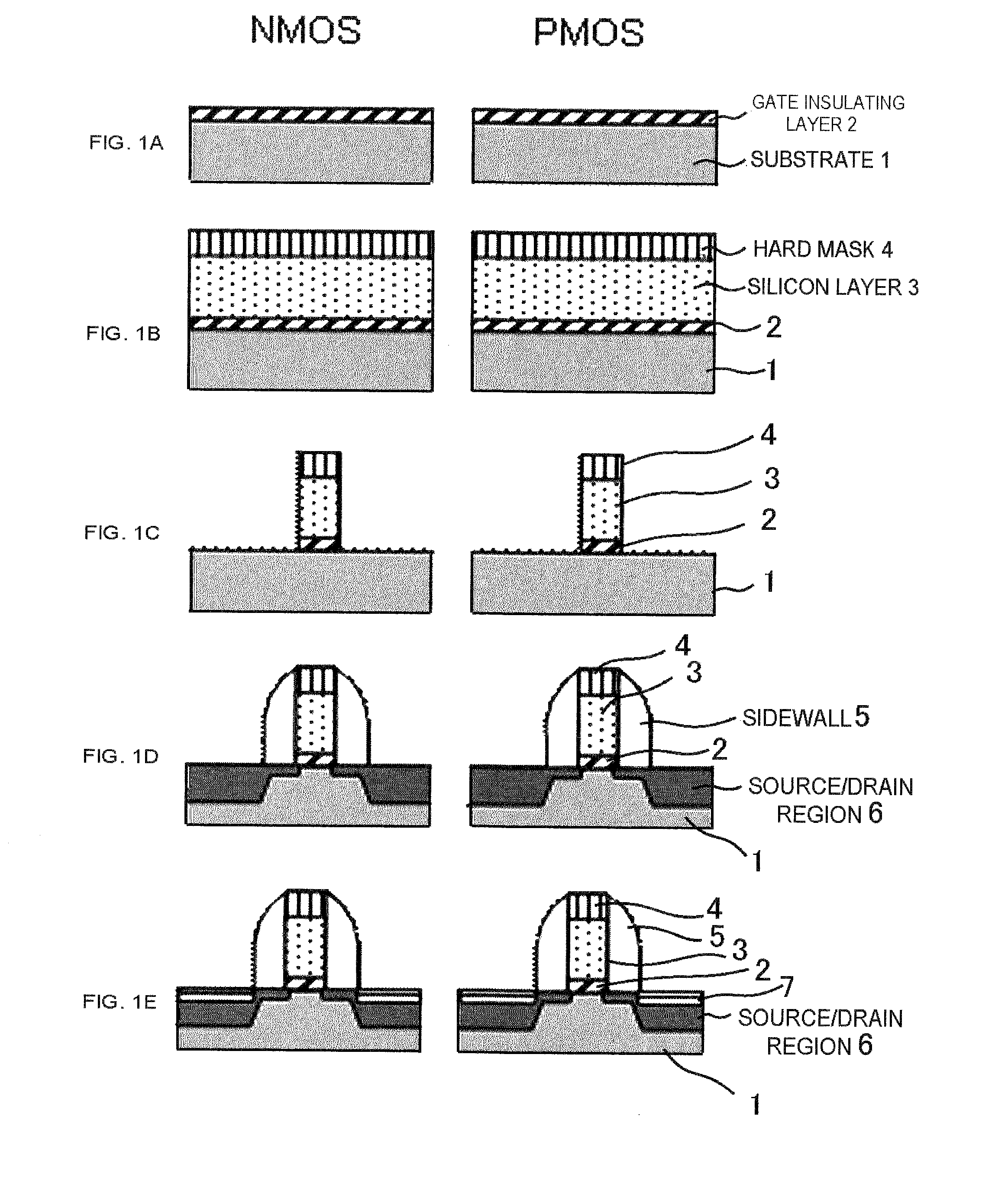
[0028]Referring to FIGS. 1A to 1E, a method of manufacturing a semiconductor device according to a first embodiment of the present invention will be described hereunder.

[0029]An oxide layer that serves as the base of a high-k gate insulating layer 2 is formed on a Si substrate 1 in a thickness of 1.0 nm by a thermal oxidation process, and a CVD process is performed so as to deposit a HfSiO layer in a thickness of 2.0 nm. The HfSiO layer is nitrided though a plasma nitriding process, to thereby form a HfSiON gate insulating layer 2 (FIG. 1A).

[0030]Then a polycrystalline silicon layer 3 is deposited on the gate insulating layer 2 in a thickness of 100 nm, and a nitride layer of 50 nm in thickness is formed as a hard mask 4 to be employed for processing the gate (FIG. 1B).

[0031]After performing a lithography process with a resist so as to process the hard mask 4, the polycrystalline silicon layer 3 and the gate insulating layer 2 are subjected to an etching process, with the hard mask ...

second embodiment

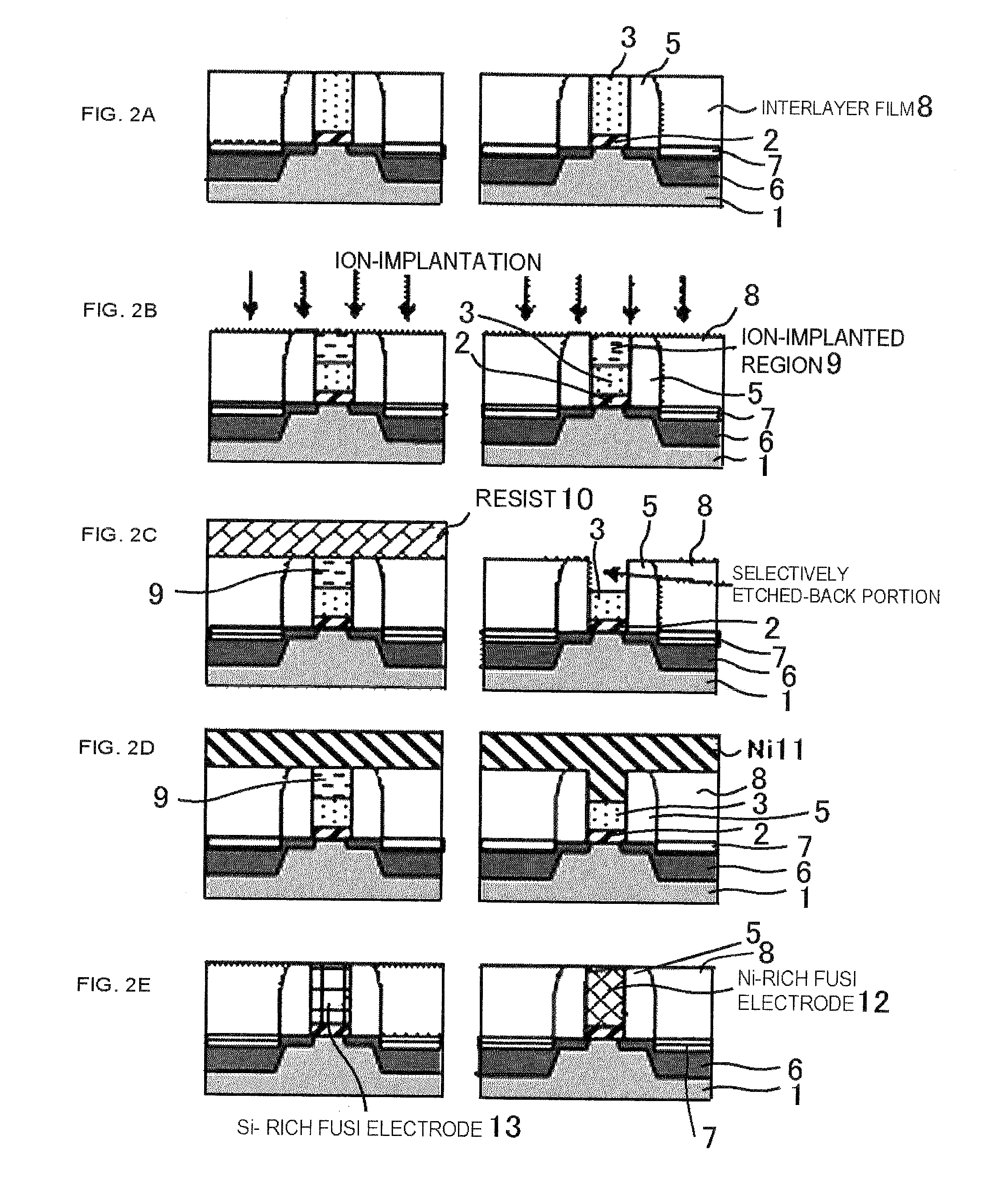
[0049]This embodiment further includes a pre-doping process, after the deposition of the polycrystalline silicon layer on the gate insulating layer in the process of the first embodiment. Referring to FIGS. 5A to 6E, such process will be described hereunder.

[0050]After forming the gate insulating layer 2 and the polycrystalline silicon layer 3 as in the first embodiment (FIG. 5A), an impurity 1 is ion-implanted into the entire surface of the polycrystalline silicon to thereby form an impurity-doped region, without performing a lithography process (FIG. 5B). In this embodiment, As is implanted at 10 keV acceleration voltage and in 3×1015 cm−2 concentration. Thereafter, similar process to the first embodiment is performed so as to process the gate with the hard mask 4, formation of the source / drain region 6, and formation of the sidewall 5. Those processes include heat treatment processes such as the activation of the source / drain impurity (generally 900° C. or higher) and substrate h...

third embodiment

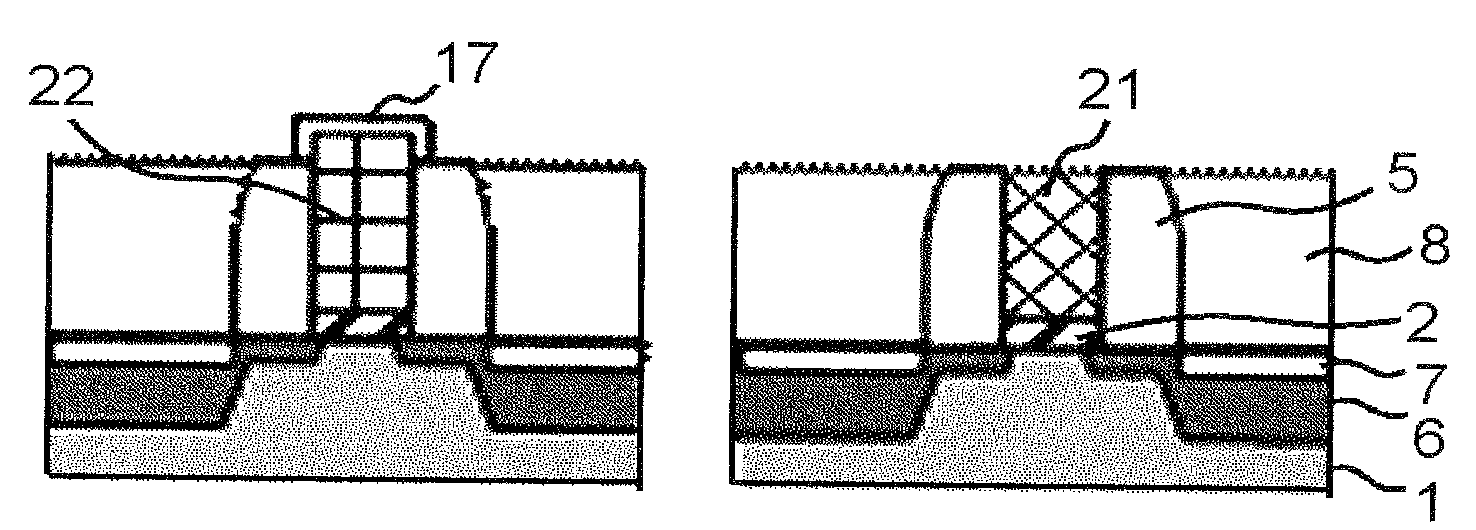
[0058]This embodiment describes an example of composition control with respect to a Ni silicide gate electrode, in the case where As is included as the impurity element implanted after exposing the upper surface of the polycrystalline silicon, referring to FIGS. 7A to 8D.

[0059]The process up to exposing the upper surface of the polycrystalline silicon layer is the same as the first embodiment, and hence the description is not repeated. After exposing the upper surface of the polycrystalline silicon layer 3 (FIG. 7A), impurity ion implantation is executed for controlling the composition of the crystalline phase of the FUSI electrode. In this embodiment, As is implanted in a concentration of 3×1015 cm−2 and at an acceleration voltage 10 keV, into the polycrystalline silicon of the gate. A majority of the As thus implanted into the polycrystalline silicon is present within a depth of 50 nm from the surface thereof (As-doped region 20 in FIG. 7B). As already stated, it is important to e...


PUM


Abstract

According to the present invention, it is provided a method of manufacturing a semiconductor device comprising a PMOS transistor and a NMOS transistor, wherein the method facilitates obtaining a FUSI phase of a suitable composition for the NMOS transistor and the PMOS transistor respectively, with fewer mask layers and through a fewer number of manufacturing steps

Description

[0001]This application is based on Japanese patent application No. 2007-065216, the content of which is incorporated hereinto by reference.BACKGROUND[0002]1. Technical Field[0003]The present invention relates to a method of manufacturing a semiconductor device, and more particularly to a method of manufacturing a semiconductor device that includes a metal-insulator-semiconductor (hereinafter, MIS) structure such as a field effect transistor.[0004]2. Related Art[0005]Investigations are being made on techniques for executing work function control or composition control of a gate electrode of a PMOS and NMOS transistor, in the attempt to better control the threshold voltage of the PMOS and NMOS transistor, which is essential for properly driving the transistor. Also, use of a metal electrode for preventing depletion of the gate electrode is currently focused on, and in particular the technique of forming a fully silicided (hereinafter, FUSI) gate electrode, which is a gate electrode tu...

Claims


Application Information

Patent Timeline
Patent Type & Authority Applications(United States)
IPC IPC(8): H01L21/28
CPCH01L21/28097H01L21/823835H01L21/823842H01L29/66545H01L29/513H01L29/517H01L29/518H01L29/4975
Inventor HASE, TAKASHI
Owner RENESAS ELECTRONICS CORP
Why Eureka
Try Eureka