Shallow trench isolation using antireflection layer

a technology of antireflection layer and trench layer, which is applied in the direction of semiconductor/solid-state device details, electrical equipment, semiconductor devices, etc., can solve the problems of increasing noise among devices on the chip, reducing the reflectivity of the entire chip, and difficulty in maintaining tight cd control, etc., to achieve the effect of reducing the reflectivity, reducing the variance of reflectivity, and simplifying the manufacturing process

Inactive Publication Date: 2006-06-13
ADVANCED MICRO DEVICES INC
View PDF30 Cites 4 Cited by
  • Summary
  • Abstract
  • Description
  • Claims
  • Application Information

AI Technical Summary

Benefits of technology

[0012]The present invention provides a method for forming shallow trench isolation among transistors and other devices on a semiconductor substrate with tight critical dimension (CD) control. Tight critical dimension control is achieved by virtue of including a highly absorbing layer of silicon rich nitride as a hardmask between a photoresist and a barrier oxide layer disposed on a semiconductor substrate. The highly absorbing layer of silicon rich nitride has an extinction coefficient (k)>0.5. As such, not only is the amount of reflectivity reduced but also the variance in reflectivity caused by thickness variations in the conventional silicon nitride layer which adversely affected photoresist patterning is significantly reduced. Also, the manufacturing process is simplified since forming of the silicon nitride layer serves as both a hardmask and an anti-reflective layer and thus no additional manufacturing step is needed to deposit an additional anti-reflective coating. In other words by using a silicon rich nitride layer as a hardmask, the cycle time for manufacturing each wafer is reduced since less manufacturing steps are needed.

Problems solved by technology

Improper isolation among transistors may cause current leakages, which can consume significant power for the entire chip.
Further, improper isolation can lead to increased noise among devices on the chip.
Unfortunately, the use of highly reflective materials such as metal silicides in photolithography has lead to difficulties in maintaining tight CD control.
In particular, undesired and nonuniform reflections from these underlying materials during the photoresist patterning process often causes the resulting photoresist patterns to be distorted.
Because the photoresist patterns are used as a mask in forming the shallow isolation trenches, such distortions have a corresponding negative impact on the CD control of these trenches.
As a result, maintaining tight CD control of the photoresist pattern and ultimately the isolation trenches is difficult.
Unfortunately, use of an ARC adds significant drawbacks with respect to process complexity.

Method used


Image

  • Shallow trench isolation using antireflection layer
  • Shallow trench isolation using antireflection layer
  • Shallow trench isolation using antireflection layer

Examples


Embodiment Construction

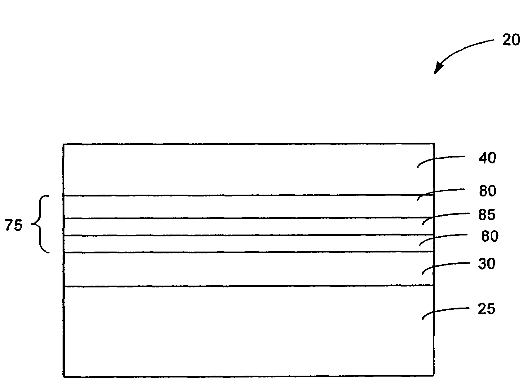
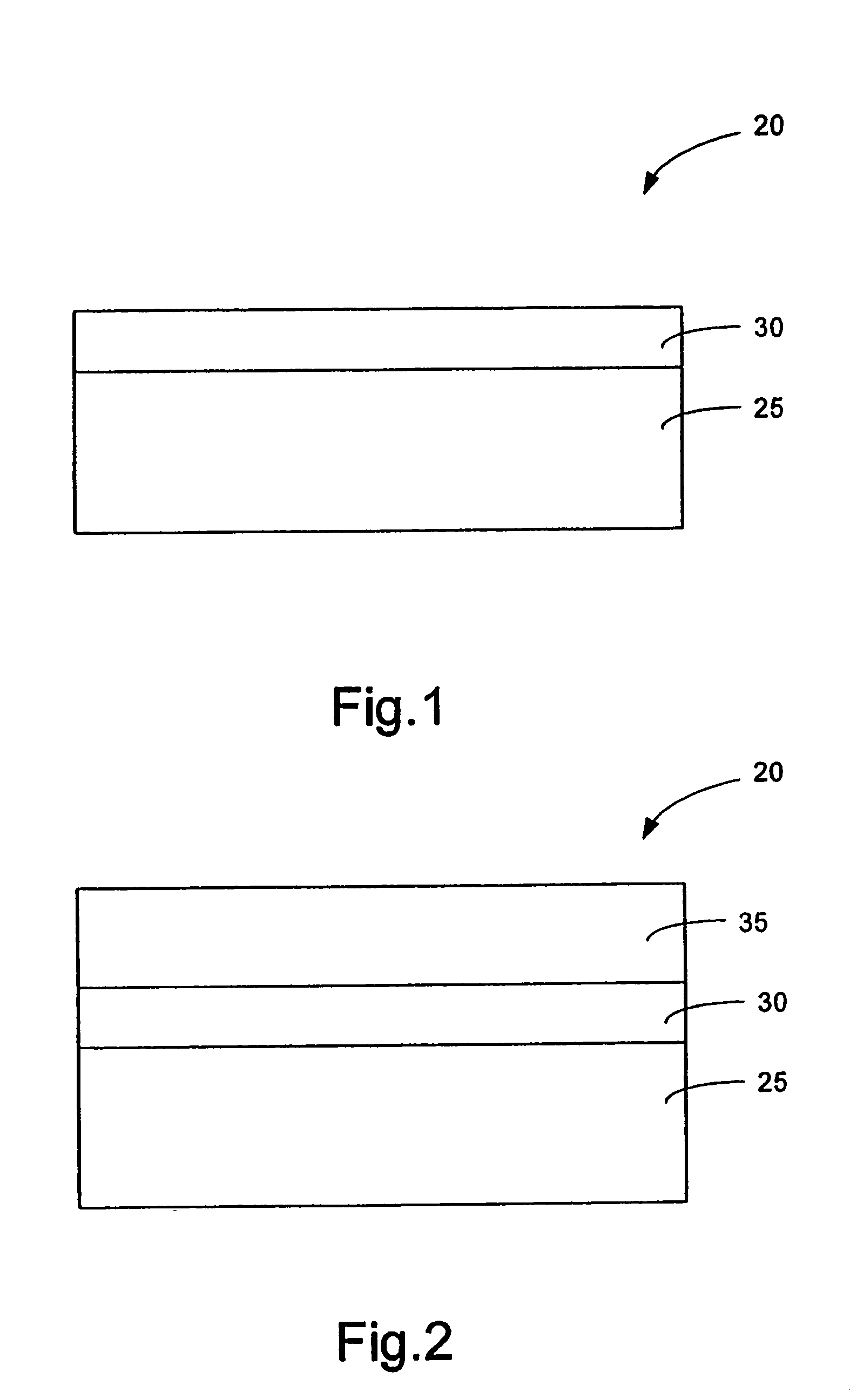
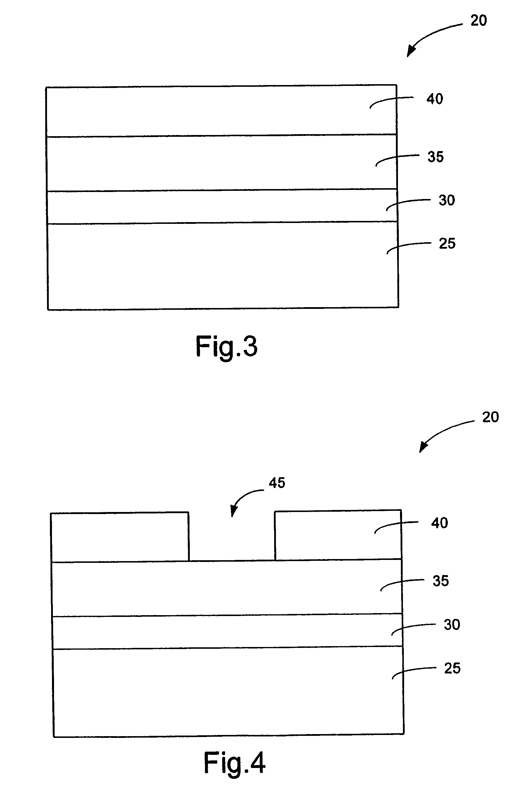
[0030]The present invention will now be described with respect to the accompanying drawings in which like numbered elements represent like parts.

[0031]In order to create shallow trench isolation (STI) among components disposed on a wafer with tight critical dimension (CD) control, the present invention provides a silicon rich nitride layer to serve as both a hardmask and an anti-reflective layer during the manufacturing process. In the present invention, the silicon rich nitride layer has a extinction coefficient (k)>0.5. By forming the hardmask of a silicon rich nitride layer, light which is reflected by the semi-conductor substrate and other material during photo-lithographic patterning of the photoresist substantially is absorbed by the silicon rich nitride layer. Thus, thickness variations in the silicon rich nitride layer do not result in non-uniform amounts of light being incident on the photoresist which in turn could result in distortions during photoresist patterning.

[0032]...


PUM


Abstract

A film stack for forming shallow trench isolation among transistors and other devices on a semiconductor substrate is provided, including a plurality of light absorbing layers alternating between a layer of SiON and a layer of SiO2 and having a combined extinction coefficient >0.5. As reflected light interacts with the light absorbing layers, a substantial amount of light is absorbed therein thereby blocking such reflected light from negatively interfering with patterning of the photoresist during photo-lithography. Following patterning of the photoresist, isolation trenches may be formed in the semiconductor substrate by etching through the light absorbing layers and into the semiconductor substrate in accordance with the pattern formed on the photoresist.

Description

CROSS REFERENCE TO RELATED APPLICATIONS[0001]The present application is a divisional of, and claims priority under 35 U.S.C. §120 to, copending, commonly assigned U.S. application Ser. No. 10 / 653,848, filed Sep. 2, 2003, now U.S. Pat. No. 6,821,883, which in turn is a divisional of, and claims priority under 35 U.S.C. §120 to U.S. application Ser. No. 09 / 861,990, filed May 17, 2001, now U.S. Pat. No. 6,645,868, which in turn is a divisional of, and claims priority under 35 U.S.C. § 120 to U.S. application Ser. No. 09 / 200,307, filed Nov. 25, 1998, now U.S. Pat. No. 6,255,717, issued on Jul. 3, 2001.TECHNICAL FIELD[0002]The present invention relates to a method for forming isolation regions among devices on a semiconductor substrate, and more particularly, to a method of patterning photoresist to form such isolation regions with reduced effects from photo-reflectivity.BACKGROUND OF THE INVENTION[0003]In the semiconductor industry, there is a continuing trend toward higher device densi...

Claims


Application Information

Patent Timeline
Patent Type & Authority Patents(United States)
IPC IPC(8): H01L21/762
CPCH01L21/76224
Inventor BABCOCK, CARL P.BHAKTA, JAYENDRA D.
Owner ADVANCED MICRO DEVICES INC
Why Eureka
Try Eureka