Self-aligned contact process enabled by low temperature

a self-aligning contact and low temperature technology, applied in semiconductor devices, semiconductor/solid-state device details, electrical apparatus, etc., can solve the problems of device malfunction, extra leakage current, and increased difficulty in pitch scaling (i.e., the space between the gate and the contact)

Active Publication Date: 2015-10-01
TESSERA INC
View PDF6 Cites 20 Cited by
  • Summary
  • Abstract
  • Description
  • Claims
  • Application Information

AI Technical Summary

Problems solved by technology

As transistor structures continue to be scaled down, the pitch scaling (i.e., the space between the gate and contact) becomes more and more challenging.
As the two contact nodes become closer to each other, the yield of the transistor is the first to be affected since the gate to contact short results in extra leakage current or even device malfunction.

Method used


Image

  • Self-aligned contact process enabled by low temperature
  • Self-aligned contact process enabled by low temperature
  • Self-aligned contact process enabled by low temperature

Examples


Embodiment Construction

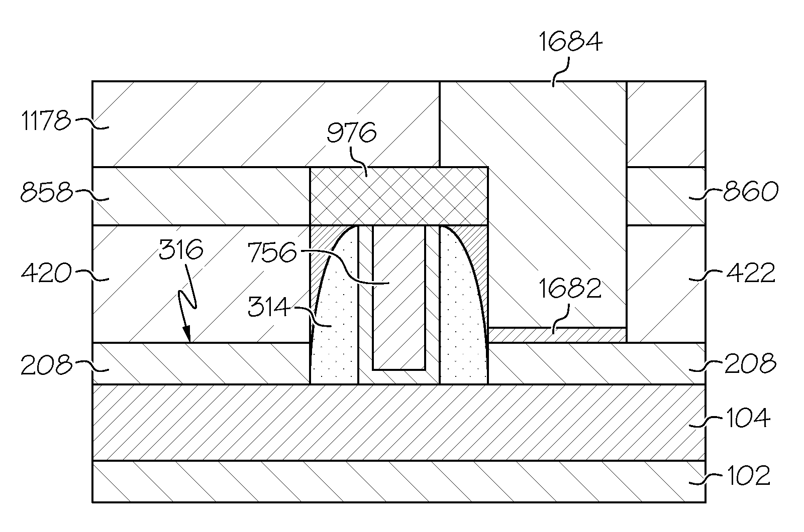
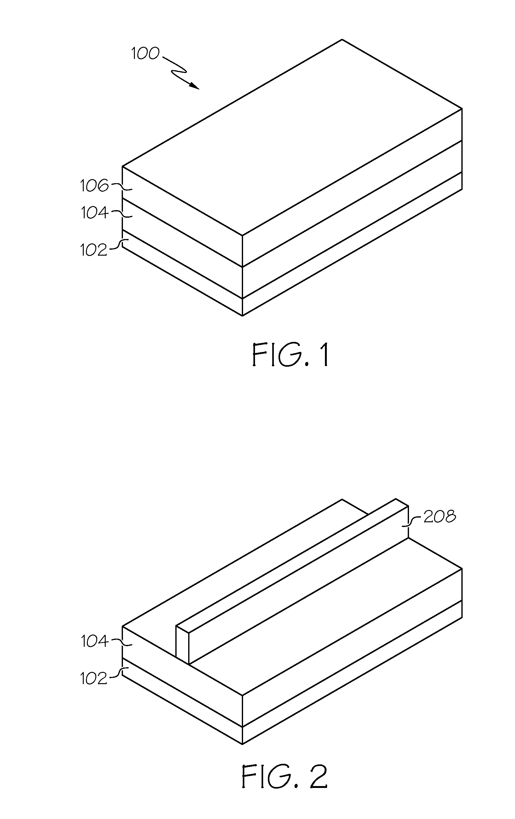
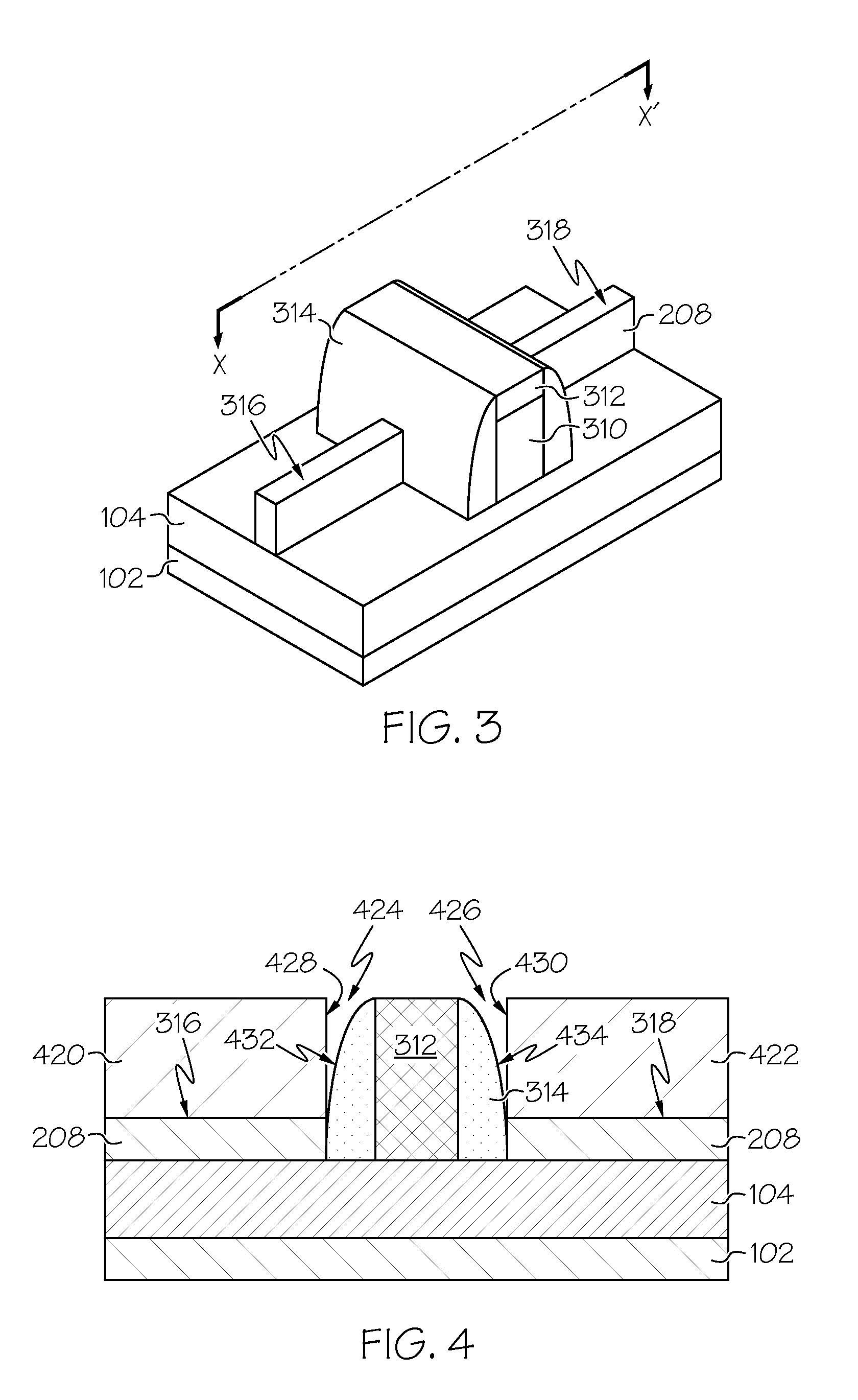
[0026]FIGS. 1 to 16 illustrate one or more processes for forming a semiconductor device with self-aligned contacts. It should be noted that although the following discussion is directed to a fin-field effect transistor (finFET), this discussion is also application to planar FETs. It should also be noted that one or more embodiments are not limited to the process for forming fin and gate structures discussed below. This discussion is provided for illustration purposes, and any process for fabricating the fin and gate structures of a finFET is applicable to embodiments of the present disclosure.

[0027]Embodiments of the present disclosure are advantageous over conventional self-aligned contact (SAC) fabrication processes and structures. In particular, one or more embodiments provide a robust SAC cap formation process without involving a gate recess. Gate recessing has been found to be a very uncontrollable process, and difficult to control the variation across the wafer. Instead of usi...


PUM


Abstract

Self-aligned contacts of a semiconductor device are fabricated by forming a metal gate structure on a portion of a semiconductor layer of a substrate. The metal gate structure contacts inner sidewalls of a gate spacer. A second sacrificial epitaxial layer is formed on a first sacrificial epitaxial layer. The first sacrificial epitaxial layer is adjacent to the gate spacer and is formed on source / drain regions of the semiconductor layer. The first and second sacrificial epitaxial layers are recessed. The recessing exposes at least a portion of the source / drain regions. A first dielectric layer is formed on the exposed portions of the source / drain regions, and over the gate spacer and metal gate structure. At least one cavity within the first dielectric layer is formed above at least one of the exposed portions of source / drain regions. At least one metal contact is formed within the at least one cavity.

Description

[0001]The present disclosure generally relates to the field of semiconductors, and more particularly relates to self-aligned contacts for semiconductor devices.BACKGROUND OF THE INVENTION[0002]As transistor structures continue to be scaled down, the pitch scaling (i.e., the space between the gate and contact) becomes more and more challenging. As the two contact nodes become closer to each other, the yield of the transistor is the first to be affected since the gate to contact short results in extra leakage current or even device malfunction.SUMMARY OF THE INVENTION[0003]In one embodiment, a method for forming self-aligned contacts of a semiconductor device is disclosed. The method comprises forming a metal gate structure on a portion of a semiconductor layer of a substrate. The metal gate structure contacts inner sidewalls of a gate spacer. A second sacrificial epitaxial layer is formed on a first sacrificial epitaxial layer. The first sacrificial epitaxial layer is adjacent to the...

Claims


Application Information

Patent Timeline
Patent Type & Authority Applications(United States)
IPC IPC(8): H01L29/78H01L21/283H01L29/66
CPCH01L29/7851H01L29/7848H01L21/283H01L29/66545H01L29/66636H01L29/66795H01L29/665H01L29/66628H01L29/165H01L21/76897H01L21/76834H01L29/41791H01L29/45H01L29/0847H01L21/76895H01L23/535H01L29/0649H01L29/66553H01L29/785
Inventor HE, HONGTSENG, CHIAHSUNYEH, CHUN-CHENYIN, YUNPENG
Owner TESSERA INC
Why Eureka
Try Eureka