Multi-junction Thin-Film Silicon Solar Cells with a Recrystallized Silicon-based Sub-Cell

a solar cell and thin film technology, applied in electrical equipment, photovoltaic energy generation, climate sustainability, etc., can solve the problems of higher crystalline silicon (e.g., microcrystalline silicon) being more expensive to deposit than lower crystalline silicon, and the impact of photovoltaic device manufacturing cos

Inactive Publication Date: 2015-10-01
OERLIKON SOLAR AG (TRUEBBACH)
View PDF0 Cites 2 Cited by
  • Summary
  • Abstract
  • Description
  • Claims
  • Application Information

AI Technical Summary

Problems solved by technology

Photovoltaic device manufacturing cost may be impacted by the degree of crystallinity.
In that, higher crystalline silicon (e.g., microcrystalline silicon) is more expensive to deposit than lower crystalline silicon (e.g., amorphous silicon).

Method used


Image

  • Multi-junction Thin-Film Silicon Solar Cells with a Recrystallized Silicon-based Sub-Cell
  • Multi-junction Thin-Film Silicon Solar Cells with a Recrystallized Silicon-based Sub-Cell
  • Multi-junction Thin-Film Silicon Solar Cells with a Recrystallized Silicon-based Sub-Cell

Examples


Embodiment Construction

[0009]Techniques disclosed herein include methods and apparatus for multi-junction solar cells that may include recrystallized silicon layers. Of course, the order of discussion of the different steps as described herein has been presented for clarity sake. In general, these steps can be performed in any suitable order. Additionally, although each of the different features, techniques, configurations, etc. herein may be discussed in different places of this disclosure, it is intended that each of the concepts can be executed independently of each other or in combination with each other. Accordingly, the concepts described in this application can be embodied and viewed in many different ways.

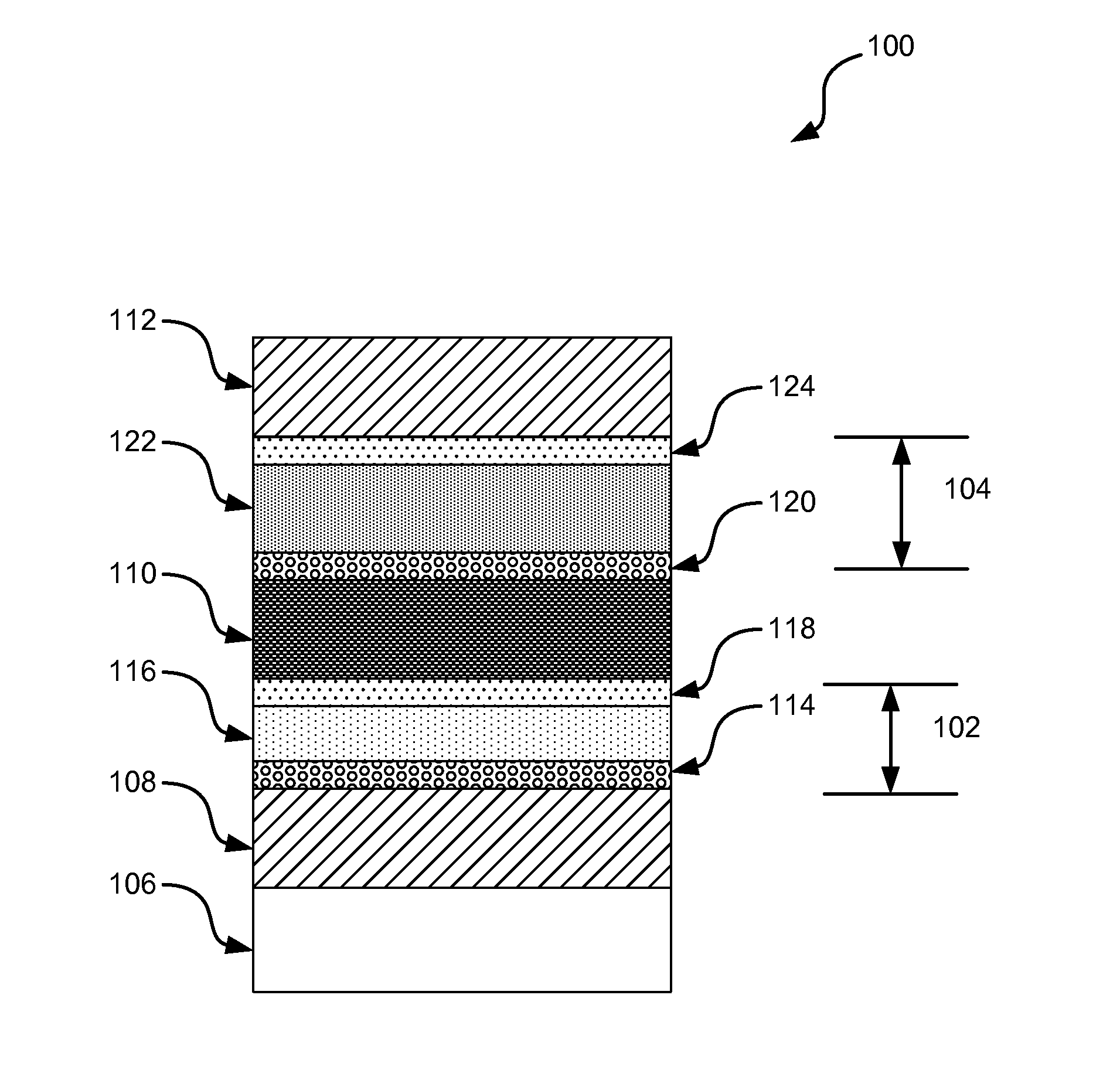
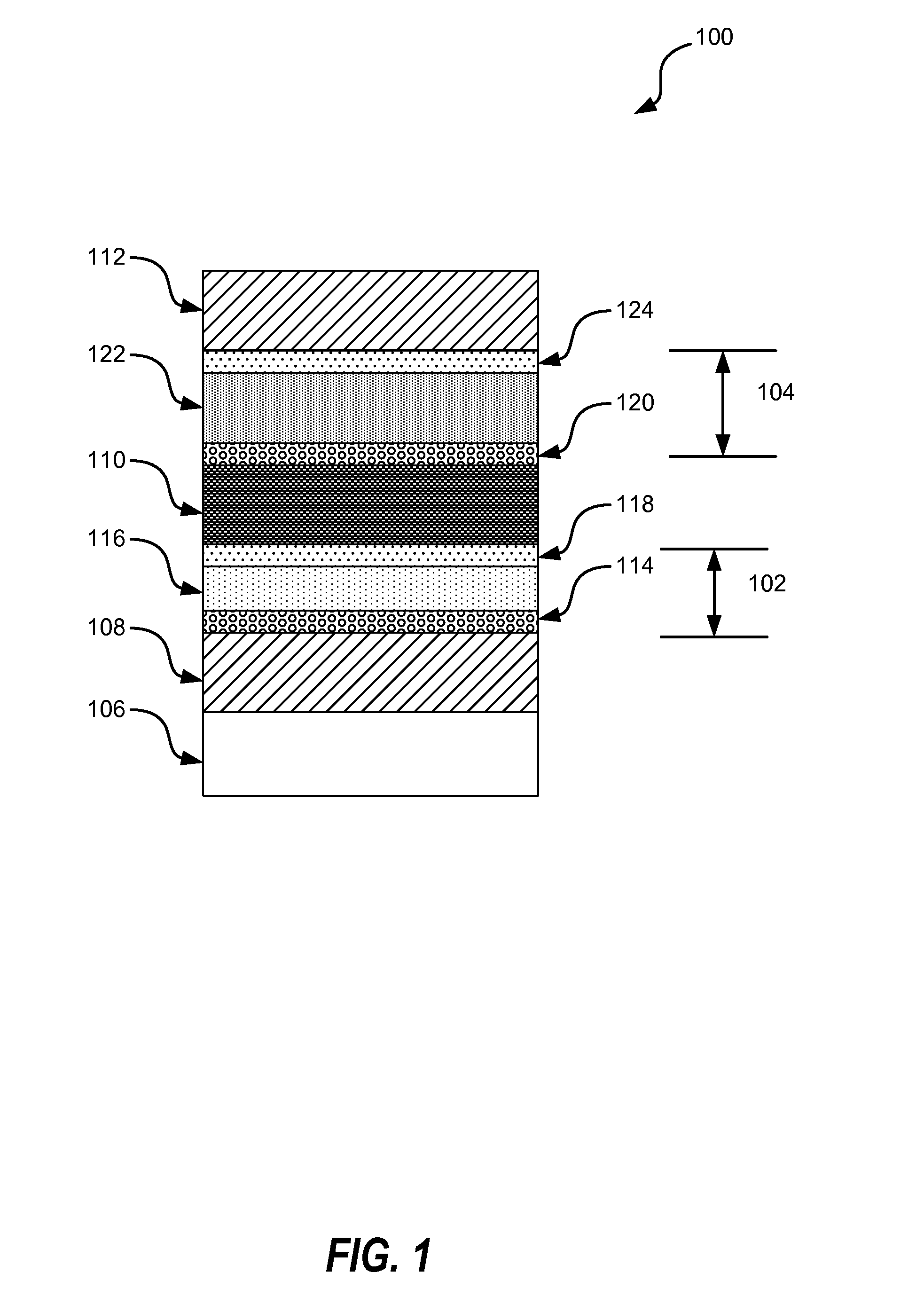
[0010]FIG. 1 illustrates a simplified diagram of a multi-junction p-i-n solar cell device 100 that may be used to convert solar radiation to electricity. Generally, solar cells may include several silicon layers that operate in concert with each other to induce electron flow within the silicon la...


PUM

PropertyMeasurementUnit
wavelengthaaaaaaaaaa
thicknessaaaaaaaaaa

Abstract

This application relates to systems and methods for multi-junction solar cells that includes at least one recrystallized silicon layer. The recrystallized silicon lay may have a microcrystalline structure following a heat treatment or laser treatment of an amorphous silicon layer. The multi-junction solar cell may be a p-i-n or n-i-p structure that may include a p-type doped silicon layer, an intrinsic silicon layer, and an n-doped silicon layer. In one embodiment, the intrinsic layer in either type of structure may be the recrystallized silicon layer.

Description

BACKGROUND OF THE INVENTION[0001]The disclosed embodiment relates generally to a method and apparatus for manufacturing a photovoltaic device, more particularly to using methods for recrystallizing silicon layer in the photovoltaic device.[0002]Silicon deposition, among other processed, may be used to manufacture photovoltaic devices that convert solar radiation into electrical energy. Silicon layers, within the photovoltaic device, may be arranged to implement the energy conversion process. The silicon-based layers may be varied based on thickness, dopant concentration, and a degree of crystallinity to control the energy conversion process. Photovoltaic device manufacturing cost may be impacted by the degree of crystallinity. In that, higher crystalline silicon (e.g., microcrystalline silicon) is more expensive to deposit than lower crystalline silicon (e.g., amorphous silicon). Accordingly, there is a desire for new and improved methods and apparatuses that enable the use of amorp...

Claims


Application Information

Patent Timeline
Patent Type & Authority Applications(United States)
IPC IPC(8): H01L31/18H01L31/20
CPCH01L31/1864H01L31/1824H01L31/202H01L31/1872H01L31/1884Y02E10/545Y02P70/50
Inventor VALLAT-SAUVAIN, EVELYNEMEIER, JOHANNES
Owner OERLIKON SOLAR AG (TRUEBBACH)
Why Eureka
Try Eureka