Display substrate and manufacturing method thereof, and flexible display device having display substrate

a flexible display device and substrate technology, applied in the field of substrates, can solve the problems of poor flexibility affecting the reliability easy damage of the display substrate of the flexible display device, so as to improve the toughness of the insulating layer, improve the reliability of the whole flexible display device, and reduce the likelihood of damage

Active Publication Date: 2015-10-08
BOE TECH GRP CO LTD
View PDF5 Cites 12 Cited by
  • Summary
  • Abstract
  • Description
  • Claims
  • Application Information

AI Technical Summary

Benefits of technology

[0020]In the display substrate, as the insulating layers are provided therein with stress absorption units, the toughness of the insulating layers is improved and the thin film transistors are less likely to be damaged when the display substrate is bent, so that the reliability of the whole flexible display device is improved.

Problems solved by technology

The insulating layers are generally made of SiNx or SiOx materials, so the insulating layers have poor flexibility.
As a result, it is likely to fracture the insulating layers when the flexible display device is bent, so that the TFTs on the display substrate of the flexible display device are easy to be damaged.
For example, the generated stress when the display substrate is bent may result in the fracture of the TFTs, so the performances of the TFTs will certainly be influenced, thereby influencing the reliability of the flexible display device and causing adverse effects on the display quality.

Method used


Image

  • Display substrate and manufacturing method thereof, and flexible display device having display substrate
  • Display substrate and manufacturing method thereof, and flexible display device having display substrate

Examples


embodiment 1

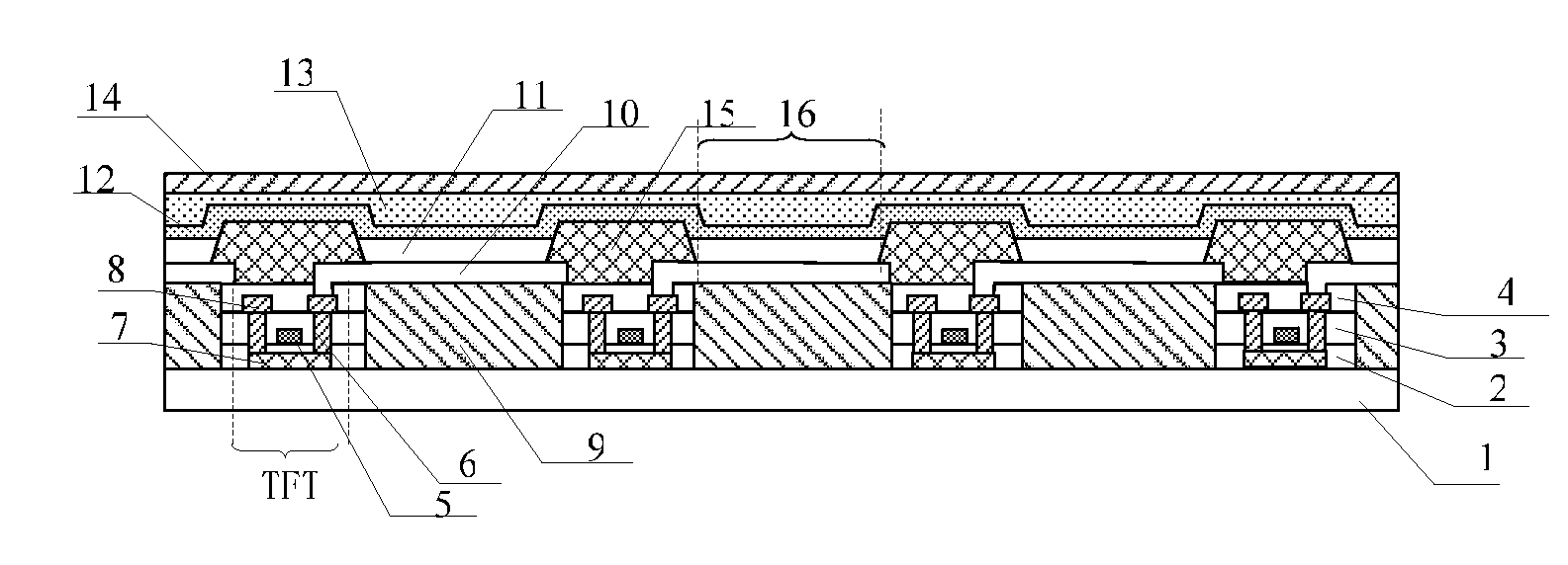
[0027]As shown in FIG. 1, this embodiment provides a display substrate, including a base substrate 1 and a plurality of thin film transistors (TFT) disposed on the base substrate 1, and further including stress absorption units 9 disposed on the base substrate 1 between adjacent thin film transistors.

[0028]A gate insulating layer 2, an interlayer insulating layer 3 and a first passivation layer 4 are also provided on the base substrate 1 in turn. These insulating layers are made of SiNx or SiOx material and thus have poor toughness, so they are likely to be fractured when the display substrate is bent. To avoid the damage to the transistors due to the fracture of the insulating layers, stress absorption units are provided in the insulating layers of the display substrate in this embodiment of the present invention.

[0029]In Embodiment 1 as shown in FIG. 1, the stress absorption units 9 are disposed in through holes penetrating through the gate insulating layer 2, the interlayer insul...

embodiment 2

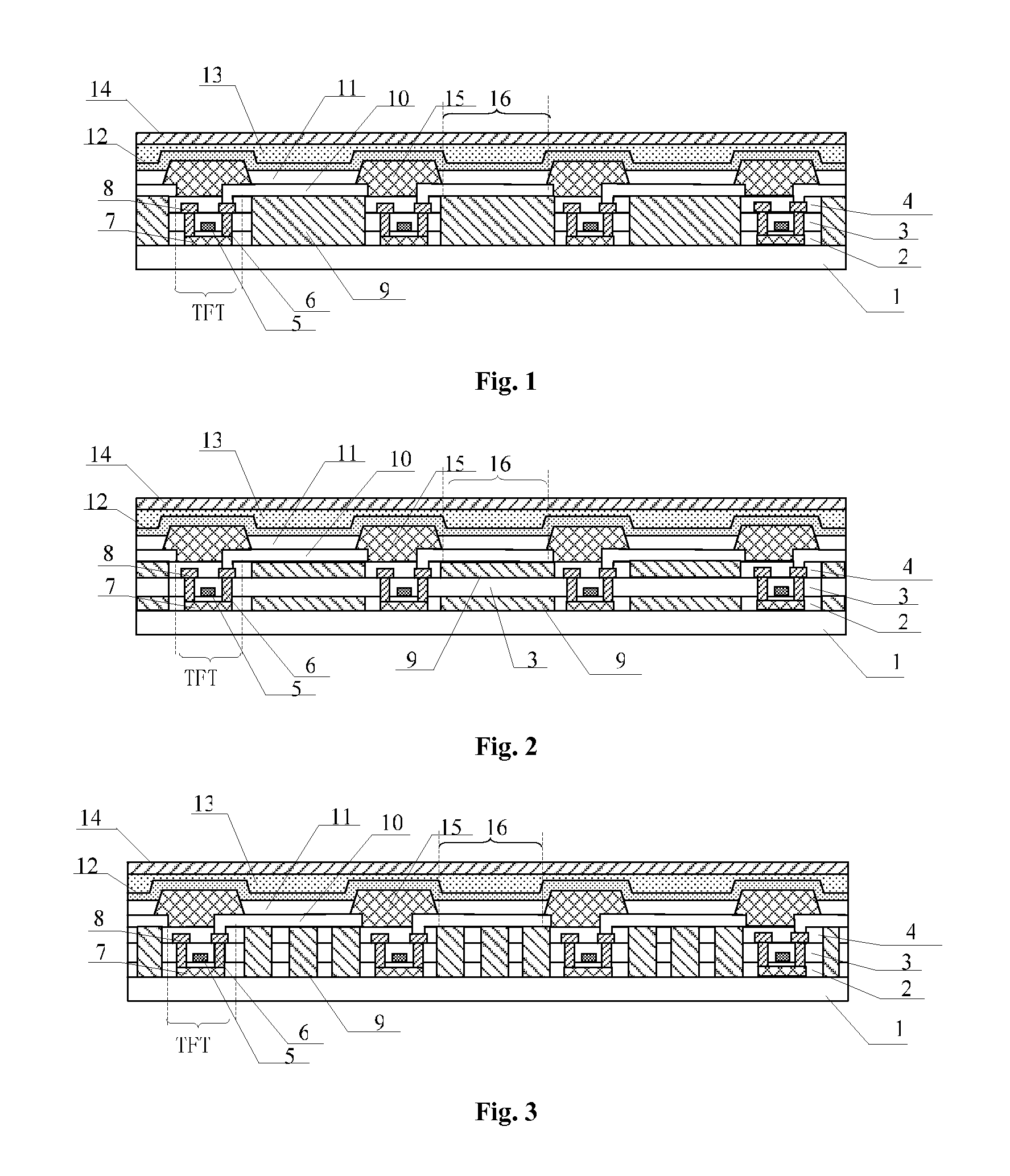
[0038]FIG. 2 shows a structural diagram of a display substrate according to Embodiment 2 of the present invention. A difference between the display substrate in this embodiment and the display substrate in Embodiment 1 lies in that: the stress absorption units 9 included in the display substrate according to Embodiment 2 of the present invention are only disposed in openings formed in the gate insulating layer 2 and the first passivation layer 4 for purpose of partially replacing the gate insulating layer 2 and the first passivation layer 4. Two stress absorption units 9 are provided on the display substrate between two adjacent thin film transistors, and the two stress absorption units 9 are spaced by the interlayer insulating layer 3 in a direction vertical to the base substrate 1. In FIG. 2, the two stress absorption units 9 between two adjacent thin film transistors are of a same size, as shown. The display substrate of such a structure may have the following advantages: as the ...

embodiment 3

[0040]FIG. 3 shows a structural diagram of a display substrate according to Embodiment 3 of the present invention. A difference between the display substrate in this embodiment and the display substrate in Embodiment 1 lies in that: in the display substrate according to Embodiment 3 of the present invention, three stress absorption units 9 are provided between two adjacent thin film transistors, and the three stress absorption units 9 are disposed in three openings penetrating through the gate insulating layer 2, the interlayer insulating layer 3 and the first passivation layer 4 and arranged at intervals in a direction parallel to the base substrate 1, for purpose of partially replacing the gate insulating layer 2, the interlayer insulating layer 3 and the first passivation layers 4. Specially, three openings penetrating through the gate insulating layer 2, the interlayer insulating layer 3 and the first passivation layer 4 are formed in the three insulating layers between two adja...


PUM


Abstract

The present invention provides a display substrate and a manufacturing method thereof, and a flexible display device having the display substrate, which belong to the field of display technology, and can solve the problem of poor reliability of display substrates due to the damage to thin film transistors when the existing display substrates are bent. In the display substrate provided by the present invention, by introducing stress absorption units made of resin material into the display substrate, the stress generated by the display substrate bent is released by the resin material, and thin film transistors on the display substrate are thus less likely to be damaged, so that the reliability of the whole display substrate is improved.

Description

FIELD OF THE INVENTION[0001]The present invention belongs to the field of display technology, and particularly to a display substrate and a manufacturing method thereof, and a flexible display device having the display substrate.BACKGROUND OF THE INVENTION[0002]Flexible display devices have many advantages, for example, impact resistance, high shock resistance, light weight, small size, convenience to carry, etc. At present, main flexible display materials may be roughly classified into three types: electronic paper (or flexible electrophoretic display), flexible Organic Light-Emitting Diodes (OLED) and flexible liquid crystals, etc.[0003]A flexible display device includes a display substrate including a flexible base substrate and a structure located on the flexible base substrate, wherein the flexible base substrate is a polyimide (PI) base substrate, a polyethylene glycol terephthalate (PET) base substrate, etc; and the structure on the flexible base substrate includes thin film ...

Claims


Application Information

Patent Timeline
Patent Type & Authority Applications(United States)
IPC IPC(8): H01L27/12H01L27/32
CPCH01L27/1248H01L27/124H01L27/1218H01L27/3244H01L27/127G02F1/133305G02F1/133345G02F2201/07G02F2201/503H10K59/12
Inventor CHENG, HONGFEIZHANG, YUXIN
Owner BOE TECH GRP CO LTD
Why Eureka
Try Eureka