Conductive via structure and fabrication method thereof

Active Publication Date: 2015-10-15
SILICONWARE PRECISION IND CO LTD
View PDF4 Cites 3 Cited by
  • Summary
  • Abstract
  • Description
  • Claims
  • Application Information

AI Technical Summary

Benefits of technology

[0024]Therefore, by filling the openings having rough wall surfaces with the dielectric layer so as to form the vias having even wall surfaces in the dielectric layer, the present invention prevents concentration of electric charges on protruding portions of the rough wall surfaces of the conductive vias as in the prior art, thereby pr

Problems solved by technology

As such, electric charges easily concentrate on protruding portions of the surfaces of the conductive vias 140, thereby easily causing joule heating under high resistance and consequently causing an open circuit to occur.
However, since copper is not compatible with the encapsulant 12, the copper seed layer easily peels off from the rough wall surfaces 130a of the openings 130, thus causing dela

Method used


Image

  • Conductive via structure and fabrication method thereof
  • Conductive via structure and fabrication method thereof
  • Conductive via structure and fabrication method thereof

Examples


Example

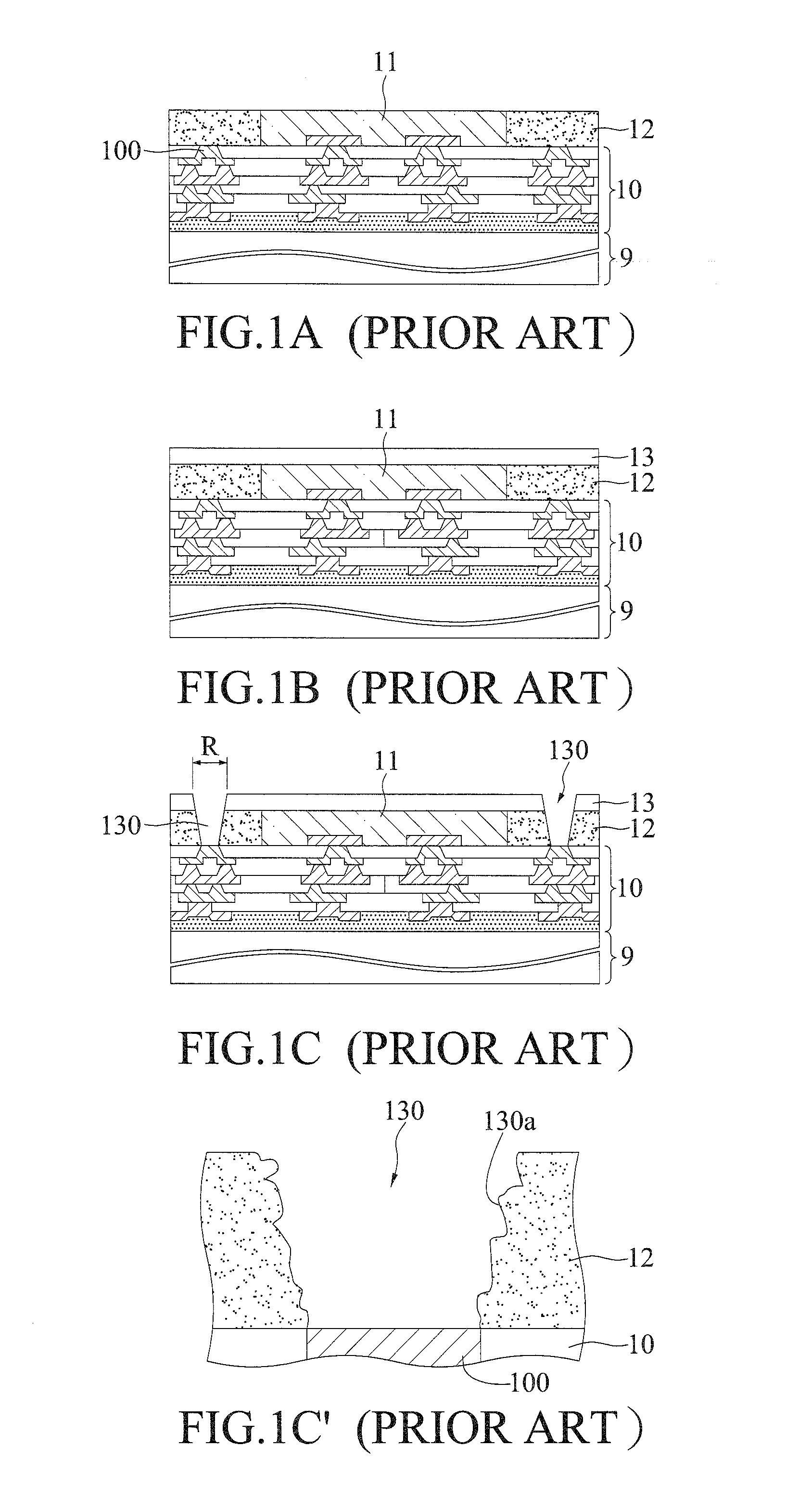
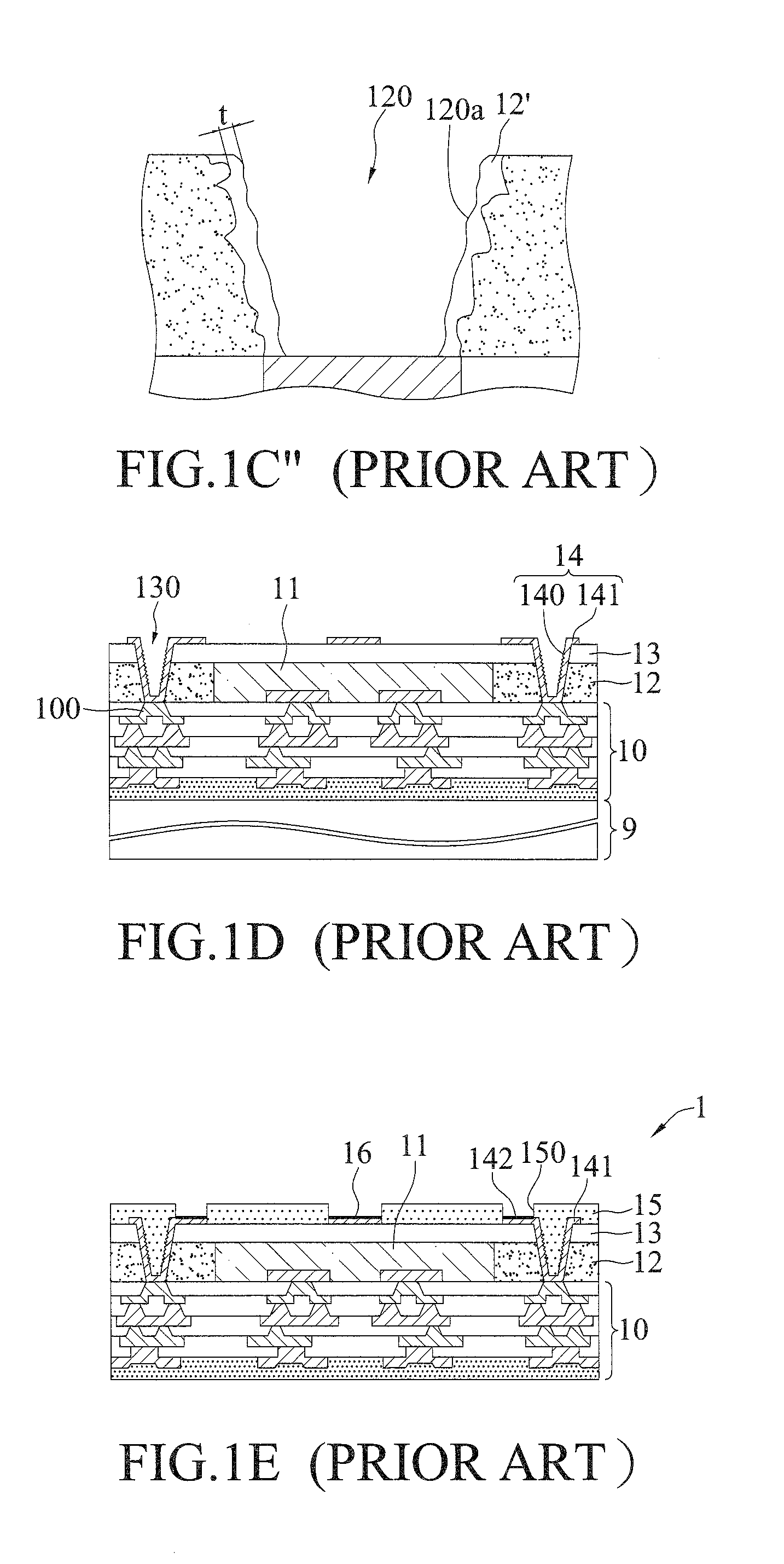
[0030]The following illustrative embodiments are provided to illustrate the disclosure of the present invention, these and other advantages and effects can be apparent to those in the art after reading this specification.

[0031]It should be noted that all the drawings are not intended to limit the present invention. Various modifications and variations can be made without departing from the spirit of the present invention. Further, terms such as “on”, “a” etc. are merely for illustrative purposes and should not be construed to limit the scope of the present invention.

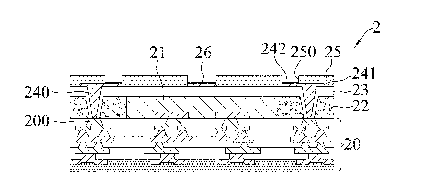
[0032]FIGS. 2A to 2D are schematic cross-sectional views showing a method for fabricating a conductive via structure according to the present invention.

[0033]Referring to FIG. 2A, a carrier 21 is disposed on a support member 9. An electronic element 21 is disposed on the carrier 20 and an encapsulant 22 is formed on the carrier 21 to encapsulate the electronic element 21. Then, a plurality of openings 220 are formed to p...


PUM


Abstract

A method for fabricating a conductive via structure is provided, which includes the steps of: forming in an encapsulant a plurality of openings penetrating therethrough; forming a dielectric layer on the encapsulant and in the openings of the encapsulant; forming a plurality of vias in the dielectric layer in the openings of the encapsulant; and forming a conductive material in the vias to thereby form conductive vias. Therefore, by filling the openings having rough wall surfaces with the dielectric layer so as to form the vias having even wall surfaces, the present invention improves the quality of the conductive vias.

Description

BACKGROUND OF THE INVENTION[0001]1. Field of the Invention[0002]The present invention relates to through molding via (TMV) technology, and more particularly, to a conductive via structure and a fabrication method thereof.[0003]2. Description of Related Art[0004]Currently, through molding via (TMV) technology has been widely applied in semiconductor fields. The TMV technology mainly involves forming openings on a surface of an encapsulant through laser ablation so as to expose electrical contacts, such as circuits or conductive pads, beneath the encapsulant.[0005]For example, the TMV technology can be used for fabricating fan-out type package on package (POP) structures. FIGS. 1A to 1D are schematic cross-sectional views showing a method for fabricating a conductive via structure for a fan-out type package on package structure according to the prior art.[0006]Referring to FIG. 1A, a packaging substrate 10 having a plurality of circuit layers 100 is disposed on a support member 9. A c...

Claims


Application Information

Patent Timeline
IPC IPC(8): H01L23/522H01L21/768H01L23/31H01L23/532
CPCH01L23/5226H01L23/53228H01L23/3107H01L21/76879H01L21/76802H01L23/49822H01L23/49827H01L23/5389H01L23/3114H01L2924/0002H01L21/76831H01L2924/00
Inventor CHEN, YAN-HENGLIN, CHUN-TANGCHI, CHIEH-YUANCHAN, MU-HSUAN
Owner SILICONWARE PRECISION IND CO LTD
Why Eureka
Try Eureka