Mold for Wiring Substrate Formation and Process for Producing the Same, Wiring Substrate and Process for Producing the Same, Process for Producing Multilayered Laminated Wiring Substrate and Method for Viahole Formation

a wiring substrate and substrate technology, applied in the direction of conductive pattern formation, contact member manufacturing, dielectric characteristics, etc., can solve the problem of requiring an extremely complicated process to produce a buildup wiring board, the quantity of heat generated by the film carrier itself due to joule heat from the wiring pattern is increased, and the process is complicated. to achieve the effect of preventing overheating the wiring board due to joule heat generated during the electrical conduction, enhancing exposing/developing accuracy,

Inactive Publication Date: 2009-12-24
MITSUI MINING & SMELTING CO LTD
View PDF0 Cites 63 Cited by
  • Summary
  • Abstract
  • Description
  • Claims
  • Application Information

AI Technical Summary

Benefits of technology

[0074]In the mold of the present invention, a desired mold pattern is formed by forming a photosensitive resin layer on a surface of a metal layer formed on a surface of a support baser then exposing and developing the photosensitive resin layer to form a desired pattern and etching the metal layer using the thus formed pattern as an etching resist. When the section of the thus formed mold pattern is observed, the sectional width of the bottom of the mold pattern on the support base side is larger than the sectional width of the top thereof.
[0075]Therefore, by pressing the mold into an uncured or semi-cured curing resin and then applying light and / or heat to the uncured or semi-cured resin introduced between the patterns formed in the mold of the present invention, the resin can be cured. In the mold pattern formed in the mold, the sectional width of the tip (top) is narrower than the sectional width of the lower end on the support base side, so that the mold of the present invention can be readily released from the cured resin after curing, and adhesion of the cured resin or the like onto the surface of the mold does not take place.
[0076]In the mold of the present invention, mold patterns of different heights can be formed by performing multistage etching of a metal layer formed on the surface of the support base, and if a curing resin layer having a thickness almost equal to the height of the highest mold pattern is formed, a depression formed by this highest mold pattern can be used as a through hole for forming a via hole in an insulating layer made of a resin cured body (film, sheet or board).
[0077]The line width of the depressed wiring pattern formed by the use of the mold of the present invention is usually not more than 10 μm, and by further enhancing exposing / developing accuracy, a wiring pattern having a line width of nanometer size can be formed. Even if the line width is narrowed as above, the depressed wiring pattern formed by the use of the mold of the present invention can be ensured to have a sectional area of a certain value or more by forming the depressed wiring pattern deeply in the thickness direction of the resin cured body (insulating layer). Consequently, by the use of the mold of the present invention, the electrical resistivity of the depressed wiring pattern formed does not become markedly high, and therefore, overheat of the wiring board due to Joule heat generated during the electrical conduction can be prevented.
[0078]In the wiring board of the present invention, a depressed wiring pattern is formed in the depth direction in the insulating layer that is formed by curing a curing resin layer. This depressed wiring pattern can be formed by transferring a mold pattern onto the curing resin layer using a mold having a desired mold pattern, said mold pattern being formed by forming a photosensitive resin layer on a surface of a metal layer formed on a surface of a support baser then exposing and developing the photosensitive resin layer to form a desired pattern and etching the metal layer using the thus formed pattern as a masking material.
[0079]That is to say, in the mold for use in the present invention, a desired mold pattern is formed by forming a photosensitive resin layer on a surface of a metal layer formed on a surface of a support base, then exposing and developing the photosensitive resin layer to form a desired pattern and etching the metal layer using the thus formed pattern as a masking material. When the section of the thus formed mold pattern is observed, the sectional shape of the mold pattern is a trapezoid wherein the bottom base width on the support base side is larger than the top base width. By allowing the mold pattern formed in the mold to penetrate into the curing resin layer, then curing the curing resin layer and releasing the curing resin cured body from the mold, a depression for forming a depressed wiring pattern can be formed in the curing resin cured body (insulating layer). As described above, the shape of the mold pattern to form a depression in the insulating layer is substantially a trapezoid, so that demolding can be easily made, and flaw of the curing resin cured body (insulating layer) hardly takes place. In particular, even if a depression of a small line width and a large depth is formed, demolding is readily made and defects hardly occur. According to the present invention, therefore, a wiring in which the wiring width is narrowed in order to increase wiring density and the wiring depth is increased in order to lower sheet resistivity can be readily formed.

Problems solved by technology

Since the thus formed ultrafine wiring pattern has a small line width and a small line thickness, the electrical resistivity given when an electric current flows tends to become large, and therefore, there occurs a problem that the quantity of heat generated by the film carrier itself due to Joule heat from the wiring pattern is increased.
Therefore, in the conventional process for producing a film carrier wherein a wiring pattern is formed by etching a metal layer that is formed on a surface of an insulating film using a conductive metal foil, there is limitation on the fining from the viewpoint of heat generation.
In the above methods, however, the step of forming a wiring pattern and the step of securing electrical connection in the thickness direction of the wiring board are completely different steps, and an extremely complicated process is required to produce a buildup wiring board.
In the conventional method to secure electrical connection in the thickness direction by forming a plating layer on the inside wall surface of the via hole, the area occupied by the via hole and its surrounding land is large, and therefore, such a conventional method can hardly cope with the recent fining and densification of wiring patterns.
In the conventional method to secure electrical connection in the thickness direction by means of via holes or bumps, it is difficult to form via holes in such a manner that they lie one upon another at the same positions in the thickness direction of the laminated wiring boards (it is difficult to form stack-up via holes).
In the above imprinting method, it is necessary to heat a resin, which is used for transferring a protrusion and a depression formed on a silicon substrate, to a temperature of not lower than the softening point of the resin and to cool the resin to a temperature of not higher than the softening point after the depression and the protrusion are transferred, so that there is a problem of a prolonged processing time.
Further, the mold used for the imprinting method is formed by, for example, etching a silicon substrate by electron beam lithography or the like, and therefore, there is a problem that when a resin film having the transferred depression and protrusion is released from the mold, a part of the resin film sometimes remains in the mold.
In the above process, however, the mold is provided with a depression and a protrusion by etching the silicon substrate surface through electron beam lithography or the like, and therefore, there resides a problem that when the mold is released from the photo-curing resin having the transferred depression and protrusion, a cured resin is liable to remain in the mold.
Also in a patent document 2 (Japanese Patent Laid-Open Publication No. 194142 / 2000), use of a photo-curing resin instead of a thermosetting resin is disclosed, but there is the same problem as above.
Therefore, even if the surface profile of the protrusion or the depression of the mold is improved, there still resides a problem that the protrusion or the depression tends to have defects when the mold is released from a resin cured body formed by introducing a resin into the protrusion or the depression of the mold.
Especially in the recent ultrafine wiring patterns, a risk of occurrence of short circuit due to running of solder is considered to become high.
In this method, however, wiring patterns of ultrafine pitch need extremely high printing alignment accuracy.
Moreover, however accurately the coating operation may be carried out, it is almost impossible to allow the actually coated portion and the coating intended portion to completely coincide with each other because the solder resist runs out.
Use of a photoresist instead of the above solder resist can be considered, but also in this method, there is limitation on the alignment accuracy of a photomask, so that this method is insufficient to produce a wiring pattern of ultrafine pitch.
However, the CSP produced by the conventional subtractive process or the like has a problem that the areas of pads including shoulders tend to become non-uniform and the heights of the molten solder balls are not equal to one another.
In the case of such CSP, further, when solder balls are arranged on pads in holes formed in an insulating film such as a polyimide film and soldered thereto, vacancies tend to be formed at the corners of the pad bottoms, and reliability about the electrical connection using solder balls sometimes becomes a problem.
In this process, however, the conductor pattern embedded in the thermoplastic resin is formed by etching a conductive metal such as a copper foil using photolithography, and therefore, this process is not suitable for producing a wiring board having a wiring pattern of ultrafine pitch.

Method used


Image

  • Mold for Wiring Substrate Formation and Process for Producing the Same, Wiring Substrate and Process for Producing the Same, Process for Producing Multilayered Laminated Wiring Substrate and Method for Viahole Formation
  • Mold for Wiring Substrate Formation and Process for Producing the Same, Wiring Substrate and Process for Producing the Same, Process for Producing Multilayered Laminated Wiring Substrate and Method for Viahole Formation
  • Mold for Wiring Substrate Formation and Process for Producing the Same, Wiring Substrate and Process for Producing the Same, Process for Producing Multilayered Laminated Wiring Substrate and Method for Viahole Formation

Examples


example 1

Preparation of Wiring Board-Forming Mold

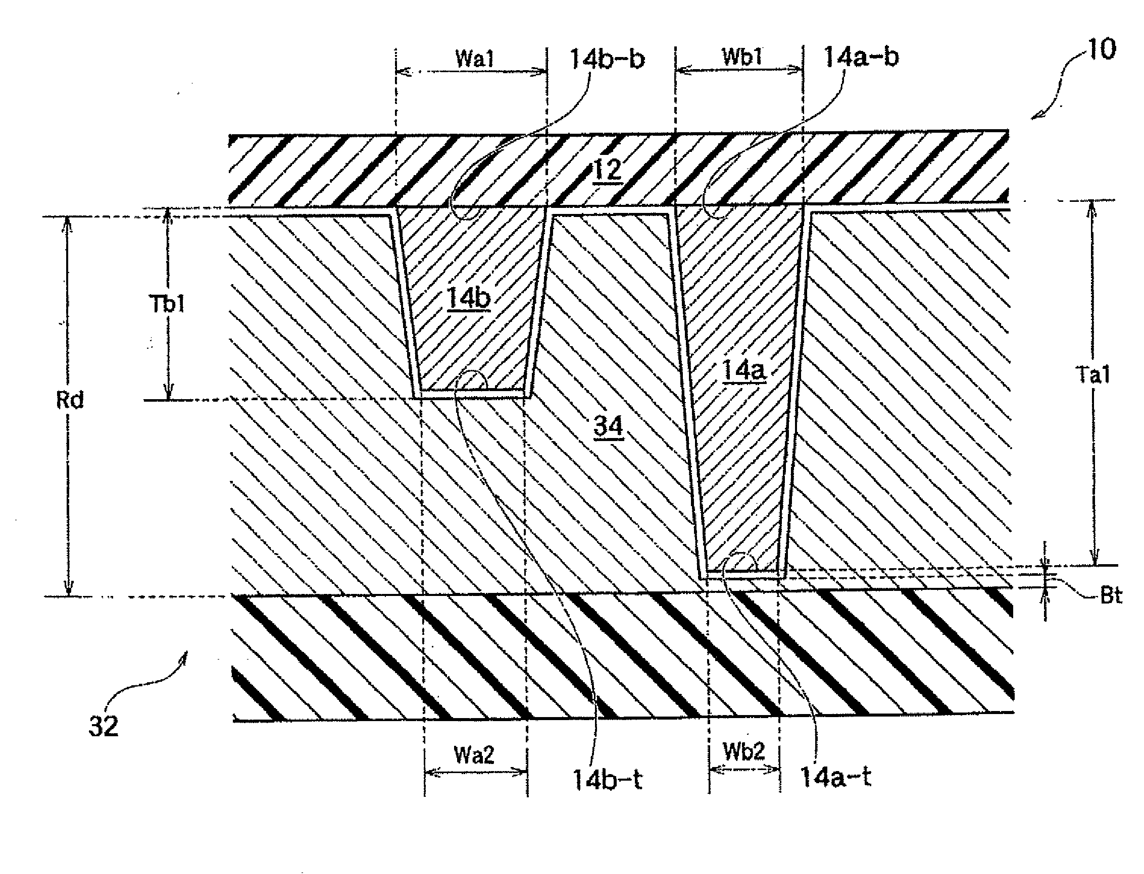
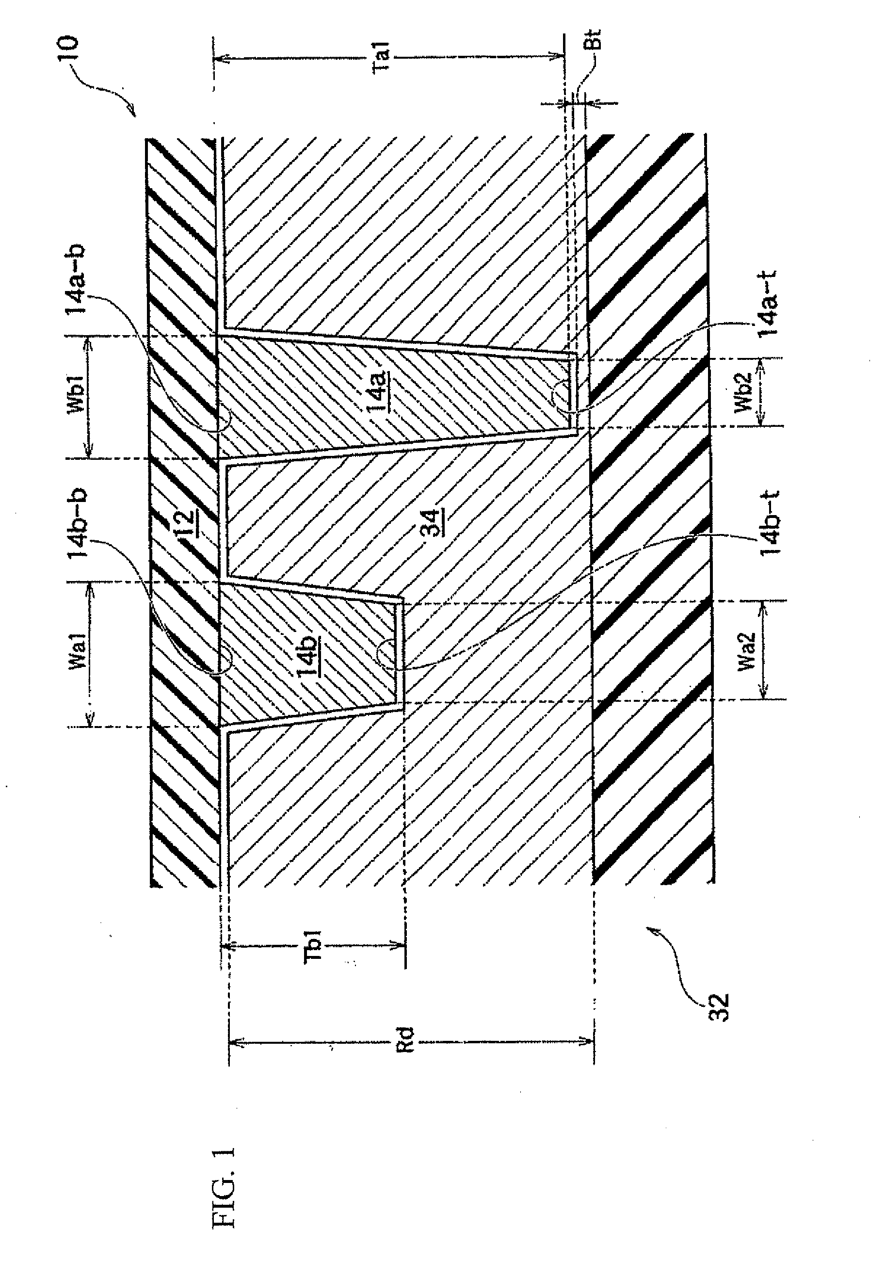
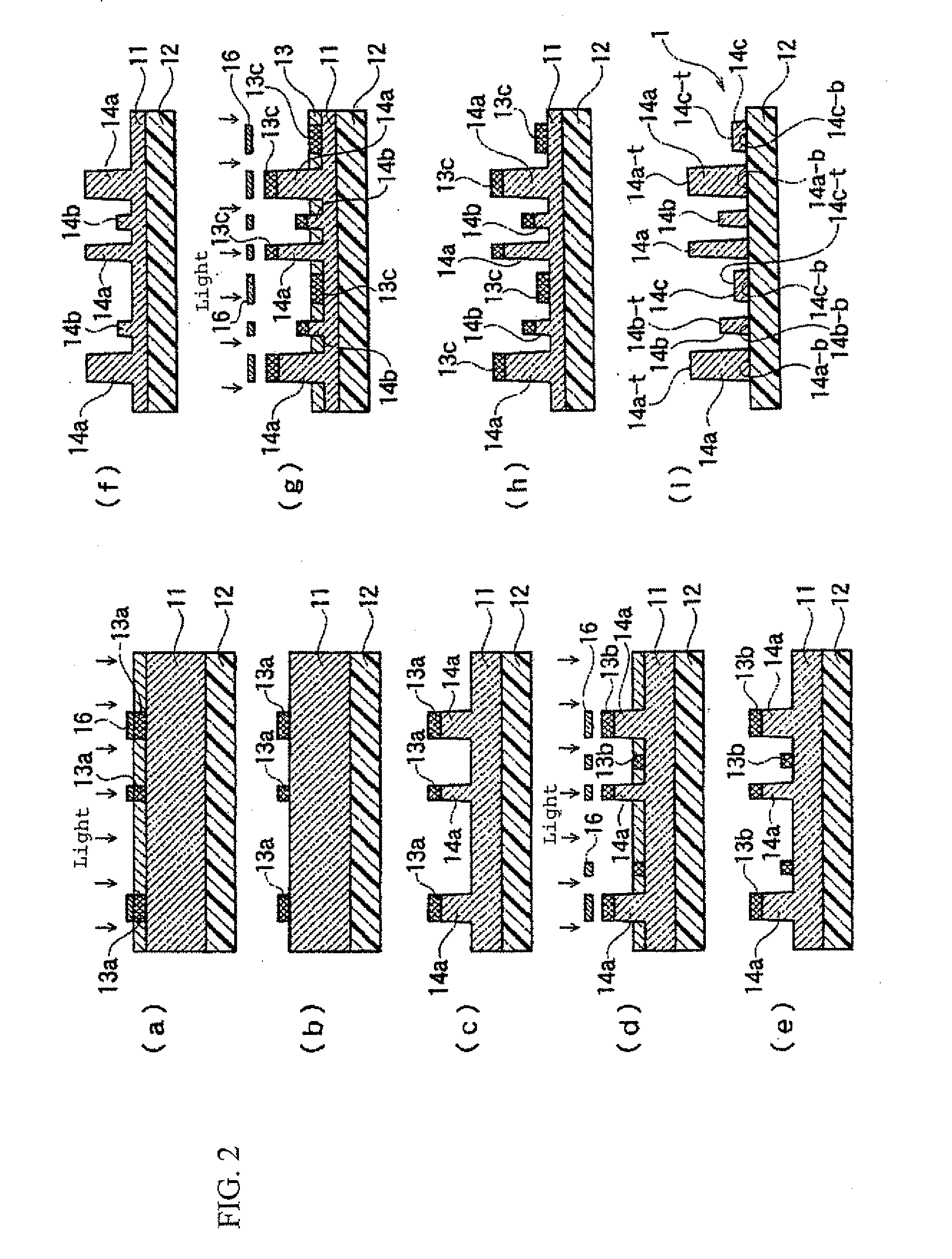
[0290]A surface of a glass substrate (support base) having a thickness of 5 mm was subjected to zincate treatment (zinc treatment) Thereafter, a nickel layer having a thickness of 0.3 μm was formed by electroless plating, and then a copper layer having a thickness of 20 μm is further formed by electroplating. On the surface of the copper layer, a photosensitive resin layer having a dry coating thickness of 2 μm was formed. On the surface of the photosensitive resin layer, a mask of a given pattern was placed, and the photosensitive resin layer was exposed to light and developed to form an etching resist made of a cured body of the photosensitive resin having a line width of 20 μm. Then, the copper layer was etched in the thickness direction by about ½ (about 10 μm) of its thickness (first etching step).

[0291]Subsequently, the masking material (etching resist, cured body of photosensitive resin) used in the first etching step was removed by an ...

example 2

[0312]On a tough pitch copper rolled copper foil having a thickness of 10 μl, a liquid crystal polymer (obtained by orientation of aromatic polyester resin) of 50 μm was laminated, and they were annealed at 180° C. for 1 hour to increase the elongation of the rolled copper foil to not less than 35% (not less than 0.35). The rolled copper foil layer of this two-layer laminate (35 mm×40 mm) was subjected to half etching in such a manner that the thickness of the rolled copper foil layer became 1 μm. The elongation e of the rolled copper foil used was 0.12.

[0313]Separately from the above, a silicon precision mold (15 mm×15 mm) having a thickness of 0.2 mm wherein a wiring pattern (rectangular) having a protrusion height of 5 μm and a pitch of 50 μm (line width: 30 μm, interval: 20 μm) had been formed was prepared.

[0314]The precision mold was disposed on the copper layer surface of the resin substrate with the copper layer of 1 μm prepared as above, and the precision mold was pressed wi...

example 3

[0321]On silicon having a size of 15 mm×15 mm, 16 protruded patterns each having a wiring height of 5 μm, a pitch of 30 μm (line width: 18 μm, interval: 12 μm) and a length of 10 mm were formed to prepare a precision mold.

[0322]Separately from the above, on a surface of a polyimide film (available from Ube Industries, Ltd., trade name: Upirex S), a Ni—Cr alloy (Cr content: 20% by weight) was sputtered in a thickness of 250 Å, and then Cu was further sputtered in a thickness of 2000 Å, to prepare an organic insulating base with a sputtering metal layer (e: about 0.15).

[0323]The precision mold was brought into contact with the sputtering metal layer surface of the organic insulating base with a sputtering metal layer prepared as above, and the precision mold was pressed with heating at 300° C. for 19.8 seconds at a pressure of 7550 g / mm2 with a heat tool of 3 mm width using a pulse heat type thermo-compression bonding device (Nippon Avionics Co. Ltd., TCW-125) to perform thermo-compre...


PUM

PropertyMeasurementUnit
thicknessaaaaaaaaaa
thicknessaaaaaaaaaa
widthaaaaaaaaaa

Abstract

A process for producing a wiring board is provided, comprising allowing a wiring board-forming mold, which comprises a support base and a mold pattern that is formed in a protruded shape on one surface of the support base wherein the sectional width of the mold pattern on the support base side is larger than the sectional width thereof on the tip side in the same section of the mold pattern, to penetrate into a curing resin layer to transfer the mold pattern, curing the curing resin layer, releasing the laminate from the mold, depositing a conductive metal, and polishing the deposited metal layer that to form a depressed wiring pattern, and a wiring board produced by this process. Further, described is a process for producing a wiring board, comprising bringing a precision mold having a mold pattern on a surface of a mold base into contact with a surface of a metal thin film formed on an organic insulating base, pressing the mold to form a depression having a shape corresponding to the mold pattern of the precision mold in the organic insulating base, thereafter forming a metal plating layer having a thickness larger than the depth of the depression to fill the plating metal in the depression, and then polishing the metal plating layer until the organic insulating base is exposed, to form a wiring pattern, and a wiring pattern produced by this process.

Description

TECHNICAL FIELD[0001]The present invention relates to a mold for forming wiring patterns of different depths in the thickness direction of an insulating resin substrate and a process for producing the mold. More particularly, the present invention relates to a process for producing a mold by selectively etching a metal layer formed on a surface of a support base, said mold being used for forming wiring patterns of different depths in the thickness direction of a curd body of a thermosetting or photo-curing resin, and also relates to the mold.[0002]Further, the present invention relates to a wiring board in which wiring patterns of different depths in the thickness direction of an insulating resin substrate are formed, a process for producing the wiring board, a process for forming a via hole, and a process for producing a multi-layer laminated wiring board. More particularly, the present invention relates to a wiring board obtained by allowing a mold, which has a mold pattern formed...

Claims


Application Information

Patent Timeline
Patent Type & Authority Applications(United States)
IPC IPC(8): H05K1/03H01K3/22H01R43/16H05K3/10H05K1/11
CPCH05K1/0265Y10T29/49204H05K3/0055H05K3/007H05K3/045H05K3/06H05K3/107H05K3/244H05K3/421H05K3/465H05K3/4682H05K2201/0108H05K2201/0317H05K2201/0352H05K2201/0382H05K2201/0394H05K2201/09563H05K2201/09727H05K2203/0108H05K2203/0152H05K2203/025H05K2203/0376H05K2203/0723H05K2203/073Y10T29/49158Y10T29/49155H05K3/0014
Inventor KAJINO, HITOSHITAGUCHI, TAKEOSATO, KANJIISHII, MASAHITOKATAOKA, TATSUO
Owner MITSUI MINING & SMELTING CO LTD
Why Eureka
Try Eureka