Multiband antenna

a multi-band antenna and antenna technology, applied in the direction of antennas, antenna details, electrical equipment, etc., can solve the problems of inefficient use of antennas only in a single band and adjacent bands

Active Publication Date: 2015-10-29
MURATA MFG CO LTD
View PDF3 Cites 15 Cited by
  • Summary
  • Abstract
  • Description
  • Claims
  • Application Information

AI Technical Summary

Benefits of technology

[0024]According to the present disclosure, since the insulation layer is provided between the radiation elements and the series passive element, the radiation elements and the series passive e...

Problems solved by technology

As such, it is inefficient to use antennas ...

Method used


Image

  • Multiband antenna
  • Multiband antenna
  • Multiband antenna

Examples


first embodiment

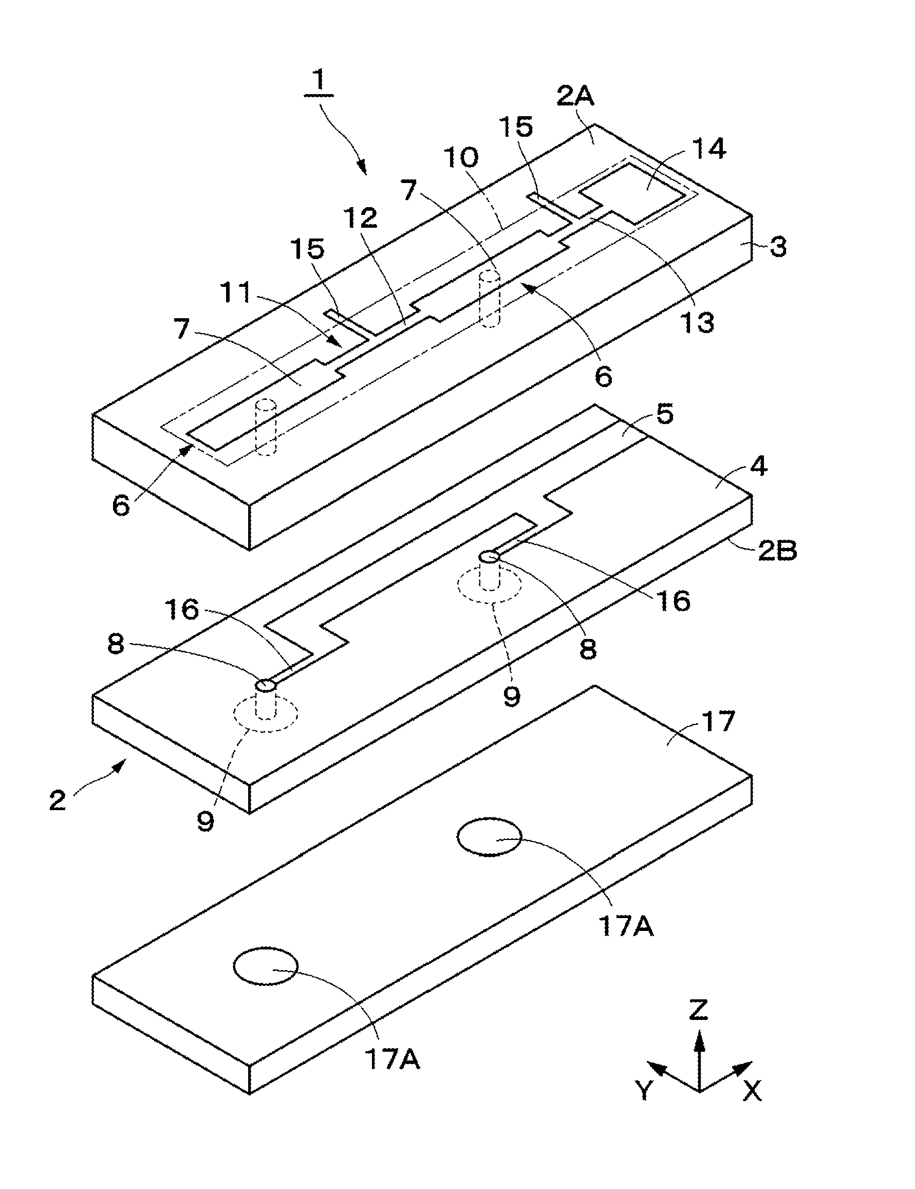
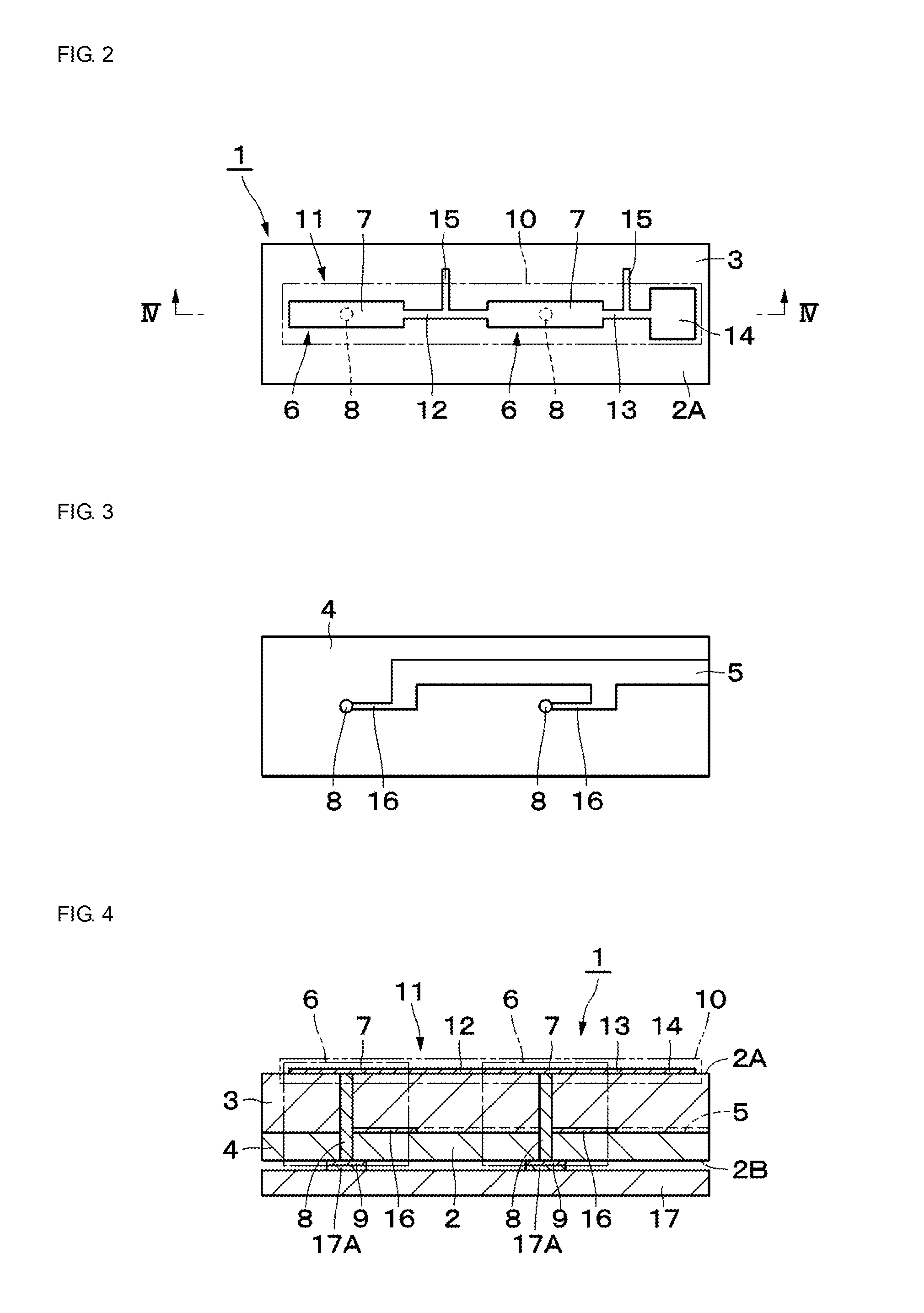
[0050]A multiband antenna 1 is shown in FIGS. 1 through 4. The multiband antenna 1 includes a multilayer substrate 2, high frequency antennas 6, a low frequency antenna 10, open stubs 15, short stubs 16, and so on.

[0051]The multilayer substrate 2 is formed in a plate shape parallel to an X-Y plane extending in an X-axis direction and a Y-axis direction among the X-axis direction, the Y-axis direction, and a Z-axis direction perpendicular to one another. The multilayer substrate 2 is a print board in which two layers, that is, thin insulative resin layers 3 and 4 are laminated as insulation layers in a direction from a front surface 2A side toward a rear surface 2B side, for example. A ground layer 5 formed with a conductive thin film of copper, silver, or the like is provided between the resin layers 3 and 4, and is connected to an external ground.

[0052]Although a resin substrate is given as an example of the multilayer substrate 2, the multilayer substrate 2 is not limited thereto...

second embodiment

[0086]The radiation element 38 is configured substantially in the same manner as the radiation element 24 and has a length dimension of a half wavelength of the high frequency signal SH in the X-axis direction, for example. The radiation element 38 is provided between the resin layers 33 and 34 of the multilayer substrate 32, and is formed with a substantially rectangular conductor pattern. The high frequency power supply line 40 that is formed of a via penetrating through the resin layers 34 and 35 is connected at a position halfway shifted in the X-axis direction from the center of the radiation element 38. The high frequency power supply line 40 is connected to the high frequency power supply unit 41 provided on the rear surface 32B of the multilayer substrate 32, and the short stub 16 is connected at a position hallway in the high frequency power supply line 40. In this case, the short stub 16 is provided between the resin layers 34 and 35 along with the ground layer 36.

[0087]T...

fifth embodiment

[0111]Note that the matching circuit is not limited to the series resonance circuit 73, and can be configured by various kinds of lumped constant circuits or distributed constant circuits. Further, although an example in which one open stub 15 is replaced with a matching circuit (series resonance circuit 73) is given in the fifth embodiment, two or more open stubs 15 may be replaced with matching circuits. In this case, switching circuits may be provided parallel to each of a plurality of matching circuits (for example, three or more matching circuits), and the length of the low frequency antenna may be changed by switching ON / OFF the respective switching circuits as needed. This makes it possible to select a plurality of frequencies.

[0112]The fifth embodiment can be applied not only to the fourth embodiment but also to the variation shown in FIG. 18, and can be further applied to a configuration in which the high frequency antenna 6 according to the first embodiment is used.

[0113]A...


PUM


Abstract

Two high frequency antennas are provided in a multilayer substrate. Each high frequency antenna is configured of a radiation element, a high frequency power supply line, and a high frequency power supply unit. A low frequency antenna is configured of a series radiation element, a low frequency power supply line, and a lower frequency power supply unit. The series radiation element is formed of two radiation elements connected by a radiation element connection line. One end side of the series radiation element is connected to the low frequency power supply unit via the low frequency power supply line. Open stubs to block transmission of a high frequency signal (SH) are connected to the radiation element connection line and the low frequency power supply line. Short stubs to block transmission of a low frequency signal (SL) are connected to the high frequency power supply lines.

Description

FIELD OF THE DISCLOSURE[0001]The present disclosure relates to multiband antennas capable of being used for a plurality of signals of different frequency bands.DESCRIPTION OF THE RELATED ART[0002]Patent Document 1 discloses a microstrip antenna (patch antenna) provided with a radiation element and a ground layer that are opposed to each other with a dielectric, which is thin in comparison with the wave length, interposed therebetween, for example, and a passive element on a radiation surface side of the radiation element. Further, Patent Document 2 discloses a planar antenna device in which two power supply points are provided in an excitation element provided on a dielectric substrate, and which is capable of radiation of two kinds of polarized waves orthogonal to each other.[0003]Patent Document 1: Japanese Unexamined Patent Application Publication No. 55-93305[0004]Patent Document 2: Japanese Unexamined Patent Application Publication No. 2004-266499BRIEF SUMMARY OF THE DISCLOSURE...

Claims


Application Information

Patent Timeline
IPC IPC(8): H01Q5/321H01Q5/10
CPCH01Q5/321
Inventor YOKOYAMA, MICHIHARUSUDO, KAORUMIZUNUMA, RYUKENNAKAJIMA, MASAYUKI
Owner MURATA MFG CO LTD
Why Eureka
Try Eureka