Antenna effect discharge circuit and manufacturing method

a discharge circuit and discharge circuit technology, applied in the direction of semiconductor/solid-state device details, diodes, semiconductor devices, etc., can solve the problems of accumulating charge on word lines, affecting the discharge circuit, and exposing the tunnel dielectric used in flash memory devices, gate dielectrics, and inter-polysilicon dielectrics to damage by accumulating charg

Active Publication Date: 2015-11-05
MACRONIX INT CO LTD
View PDF5 Cites 13 Cited by
  • Summary
  • Abstract
  • Description
  • Claims
  • Application Information

AI Technical Summary

Problems solved by technology

Antenna effect induced charges may damage structures in the device, including structures critical to device performance.
For example, in memory devices, word lines or other relatively large conductive structures can suffer significant charge accumulation due to the antenna effect.
Charge accumulation on the word lines can expose tunnel dielectrics used in flash memory devices, gate dielectrics, and inter-polysilicon dielectrics, to damage by the accumulated charge.
Furthermore, charge storage structures utilized in dielectric charge storage cells can be particularly susceptible to this kind of damage.
However, both methods have limitations.
Moreover, the PN diode only provides protection after breakdown voltage, thus it cannot protect the medium-range voltages.
The fuse protection is only suitable for small test device, but not suitable for a product design.
Besides, if the rupture bias is too large it may disturb the device as well.
However, ESD circuits are often activated under relative highs voltage and cannot provide a medium-voltage protection.

Method used


Image

  • Antenna effect discharge circuit and manufacturing method
  • Antenna effect discharge circuit and manufacturing method
  • Antenna effect discharge circuit and manufacturing method

Examples


Embodiment Construction

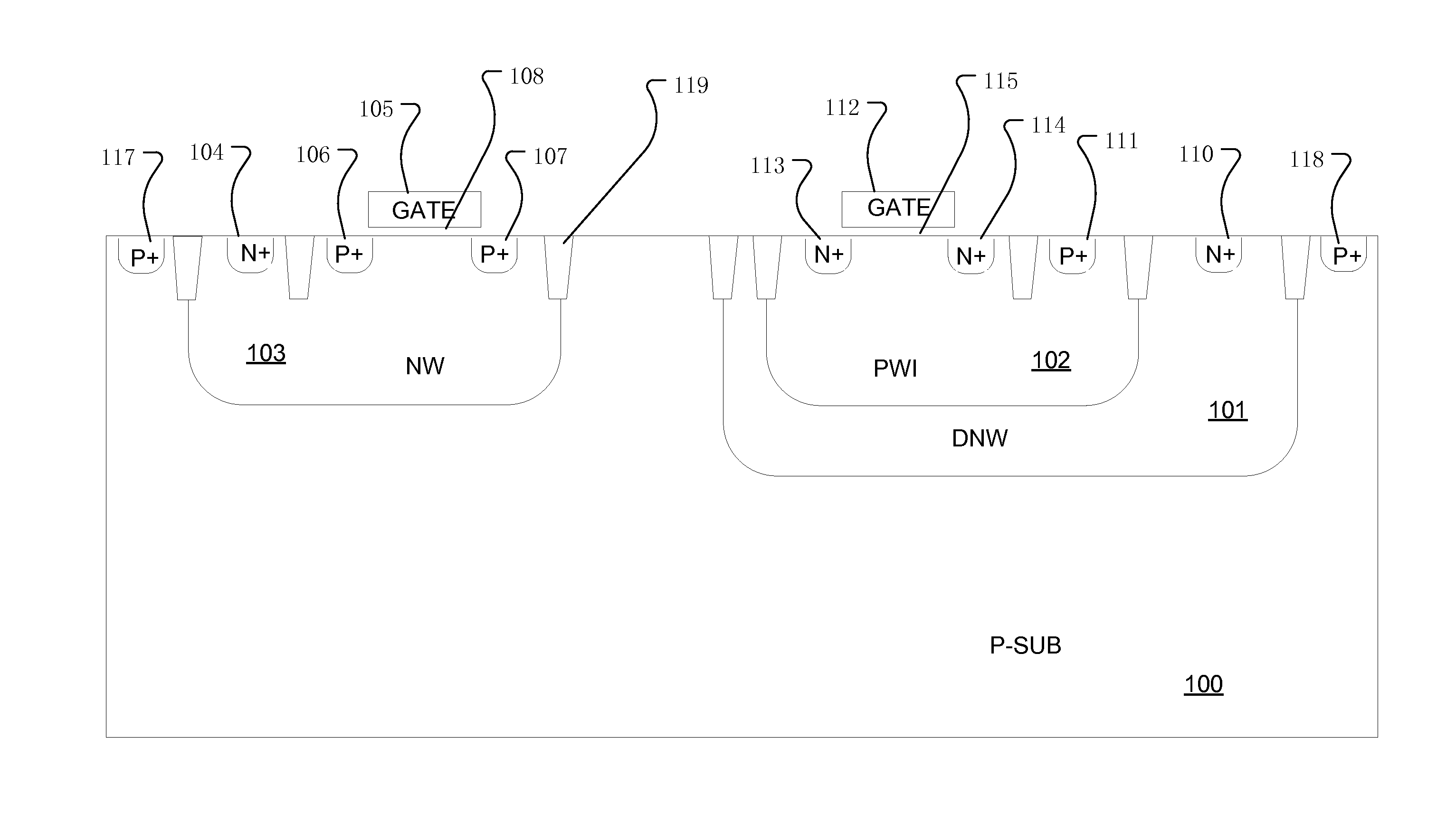
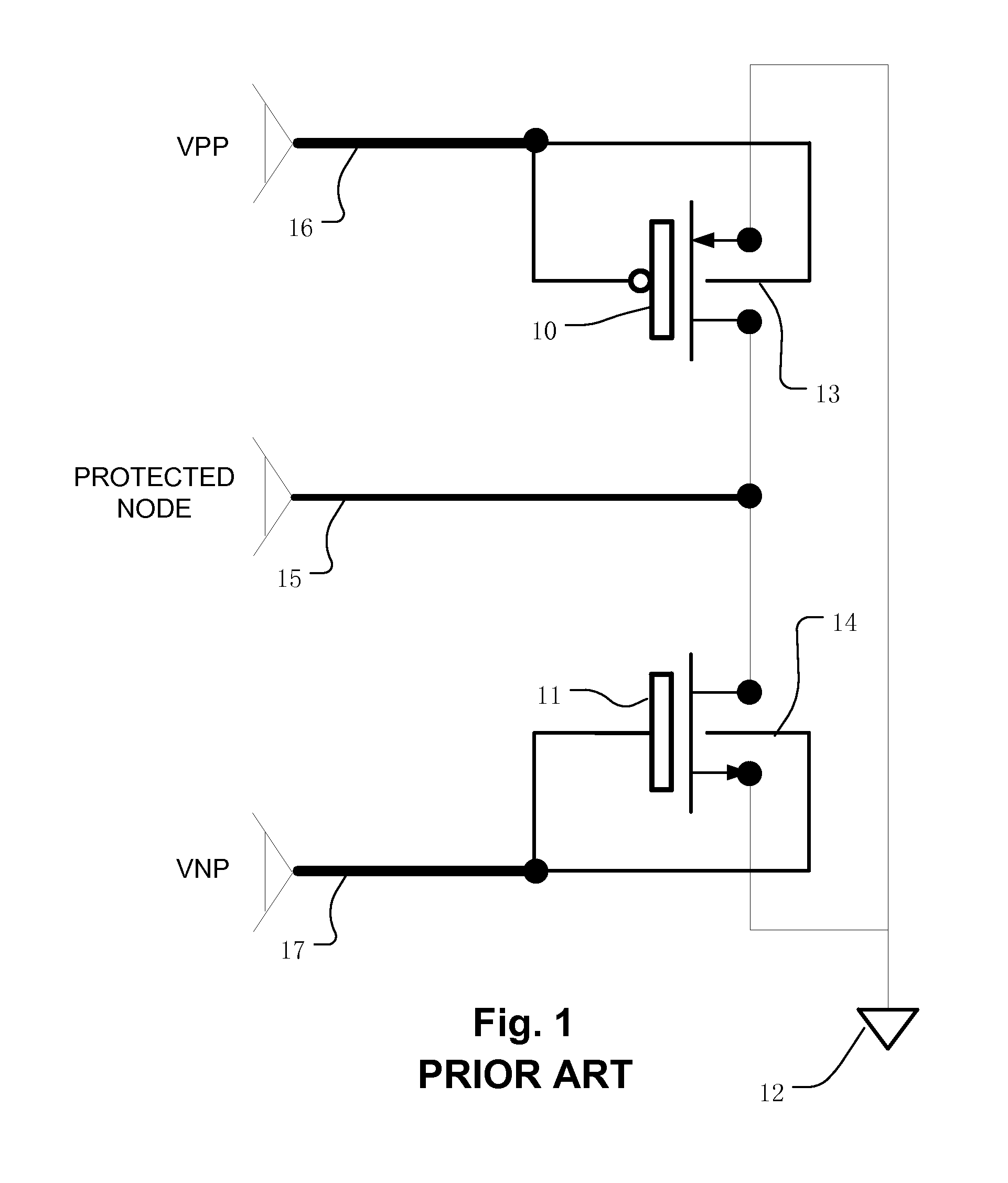
[0037]A detailed description of embodiments of the present invention is provided with reference to the FIGS. 1-20.

[0038]FIG. 1 illustrates a prior art protection circuit for the antenna effect, based on a dynamic threshold MOS pair of transistors 10, 11. The drain of the PMOS transistor is coupled to the substrate ground 12. Likewise, the drain of the NMOS transistor 11 is coupled to the substrate ground 12. The channel well 13 in the channel region of the PMOS transistor is connected to the gate of the PMOS transistor using a lower patterned conductor, like the first metal layer. Likewise, the channel well 14 in the channel region of the NMOS transistor 11 is connected to the gate of the NMOS transistor 11 using a lower patterned conductor, like the first metal layer. The sources of the PMOS transistor 10 and the NMOS transistor 11 are connected to the node 15 that is to be protected from the charge buildup caused by the antenna effect.

[0039]The terms “source” and “drain” are often...


PUM


Abstract

An antenna effect discharge circuit is described for a device having patterned conductor layers, which may be exposed to charge inducing environments during a manufacturing process. The antenna effect discharge circuit has a terminal that is connected to a node on the device to be protected from charge accumulation and a gate, such as the gate of a field effect transistor in the circuit, and a terminal through which accumulated charge can be discharged to the substrate. A capacitor couples the gate in the antenna effect discharge circuit to the substrate. A voltage supply circuit is configured to provide voltage sufficient to bias the antenna effect discharge circuit in an off condition during operation of the device. A patterned conductor in the upper layer, and preferably the uppermost layer, of the device links the gate in the antenna effect discharge circuit to the voltage supply circuit.

Description

BACKGROUND[0001]1. Field of the Invention[0002]The present invention relates to integrated circuit structures which address charge accumulation during manufacture.[0003]2. Description of Related Art[0004]In the manufacturing of integrated circuits, some processes utilize activated ions. For example, backend processes including metal etching, photoresist stripping, and deposition of inter-metal dielectrics, involve plasmas which induce charge on the structures in the die being treated. This charging of structures during manufacturing can be referred to as the antenna effect.[0005]Antenna effect induced charges may damage structures in the device, including structures critical to device performance. For example, in memory devices, word lines or other relatively large conductive structures can suffer significant charge accumulation due to the antenna effect. Charge accumulation on the word lines can expose tunnel dielectrics used in flash memory devices, gate dielectrics, and inter-pol...

Claims


Application Information

Patent Timeline
Patent Type & Authority Applications(United States)
IPC IPC(8): H01L27/02H01L23/552H01L21/8238H01L27/06
CPCH01L27/0266H01L21/823871H01L23/552H01L27/0629H01L27/0292H01L2924/0002H10B43/40H10B43/27H01L2924/00
Inventor LUE, HANG-TINGYEH, TENG-HAO
Owner MACRONIX INT CO LTD
Why Eureka
Try Eureka