

High sensitivity testing structure for evaluating plasma antenna effect
A testing structure and plasma technology, which is applied in semiconductor/solid-state device testing/measurement, electric solid-state devices, semiconductor devices, etc., can solve the problems of insufficient detection sensitivity of charge monitoring chips, complex structure of charge monitoring chips, and high manufacturing costs.
- Summary
- Abstract
- Description
- Claims
- Application Information
AI Technical Summary
Problems solved by technology
Method used
Image

Examples
Embodiment Construction
[0024] As mentioned earlier, the existing E 2 One of the disadvantages of the charge monitoring chip with PROM structure is that two polysilicon stacked layers need to be fabricated, that is, the floating gate and the control gate structure must be defined separately. Therefore, at least one additional photolithography and etching process and cleaning steps are required in the manufacturing process, resulting in an increase in cost. In addition, more sensitive test structures are needed to evaluate the plasma-derived charges accumulated on the wafer surface. The test structure of the invention has the advantages of high sensitivity, low manufacturing cost and quantitative analysis, and can completely make up for the deficiencies of the prior art.
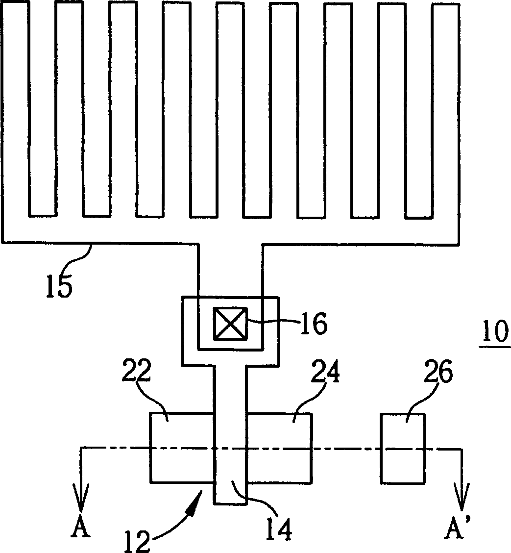
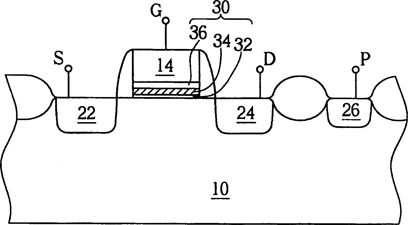
[0025] see figure 1 , figure 1 It is a schematic top view of the test structure of the present invention. Such as figure 1 As shown, a field effect transistor 12 is provided on a substrate 10 . The substrate 10 is made of a si...
PUM
| Property | Measurement | Unit |
|---|---|---|
| Thickness | aaaaa | aaaaa |
| Thickness | aaaaa | aaaaa |
| Thickness | aaaaa | aaaaa |
Abstract
Description
Claims
Application Information